产品型号带"Z"表示符合RoHS标准。评估此电路需要下列选中的电路板Conductivity and Total Dissolved Solids TheoryThe TDS in a solution is largely composed of inorganic salts that separate into ions in the presence of a polar solvent like water. When a potential is applied to the solution via two electrodes, the movement of the ions constitutes a current that, when there is negligible electrolysis, obeys Ohm’s law. The resistance, R, of the solution can then be calculated by Equation 1.
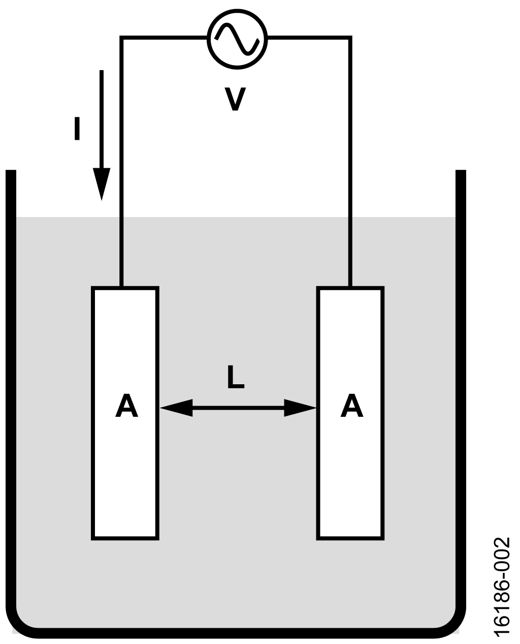
where: V is the potential difference applied to the two electrodes. I is the measured current across the two electrodes. ρ is the resistivity of the material in Ω cm. L is the distance between the two electrodes. A is the area of the electrodes.
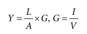
The conductance, G, is the reciprocal of resistance and measured in Siemens (S), and conductivity, Y, is the reciprocal of resistivity and measured in S/cm, mS/cm, or µS/cm. Rearranging Equation 1, the conductance can be obtained from the potential across the two electrodes and the current through them. Conductivity is the conductance multiplied by a factor related to the geometry of the electrodes (see Equation 2).
Typically, conductivity is measured using a 2-electrode sensor called a conductivity probe or conductivity cell. An excitation voltage is applied to the conductivity cell while it is immersed in the solution as shown in Figure 2.
The conductivity cell constant or simply cell constant, KCELL, is the ratio of the gap between its two electrodes and the area of each electrode, which shortens Equation 2 to Equation 3. The cell constant has a unit of cm−1 but the unit may be omitted by manufacturers of conductivity probes.
The typical measurement system computes conductance from the current and voltage readings. Since the conductivity range of values is very large, measuring conductance at the extremes (values less than 1 µS and greater than 0.1 S) can be difficult for ordinary instruments. By choosing a conductivity cell with an appropriate cell constant, the range of conductivity measurement can be extended. Conductivities less than 0.1 µS/cm can be measured at a lower conductance by using a conductivity cell with a lower cell constant. Conversely, conductivities greater than 0.1 S/cm can be measured at a higher conductance by using a conductivity cell with a higher cell constant. Typical values of the cell constant used for a corresponding range of conductivity measurement is shown in Table 1.
Each conductivity cell has a rated excitation voltage, which must not be exceeded so as not to damage the electrodes. Do not apply a dc voltage to any of the electrodes.
Dielectric PropertiesPolarization and the dielectric properties of the solution primarily affect the accuracy of the measured voltage signal across and the current through the conductivity cell. Polarization arises from the accumulation of ions and the chemical reactions that occur near the electrode surface. The dielectric properties of the solution contribute to a frequency dependent impedance and interelectrode capacitance. A technique used to maximize the accuracy of the conductance measurement uses a bipolar pulse excitation. An excitation voltage +VEXC is applied for time t1 then the opposite excitation voltage −VEXC is applied for time t2. Also, t1 and t2, and +VEXC and −VEXC must be equal with no greater than 1% difference in duration and magnitude, respectively. The frequency of the signal (t1 + t2) −1 must be adjusted to the range of conductance measurement. Typically, this is 94 Hz in the µS range and 2.4 kHz in the mS range. These frequencies are compromises that minimize the effect of interelectrode capacitance, while preventing the accumulation of ions on the electrode surface.
Conductivity MeasurementThe front-end of the conductivity measurement can be simplified to a voltage divider network as shown in Figure 3.
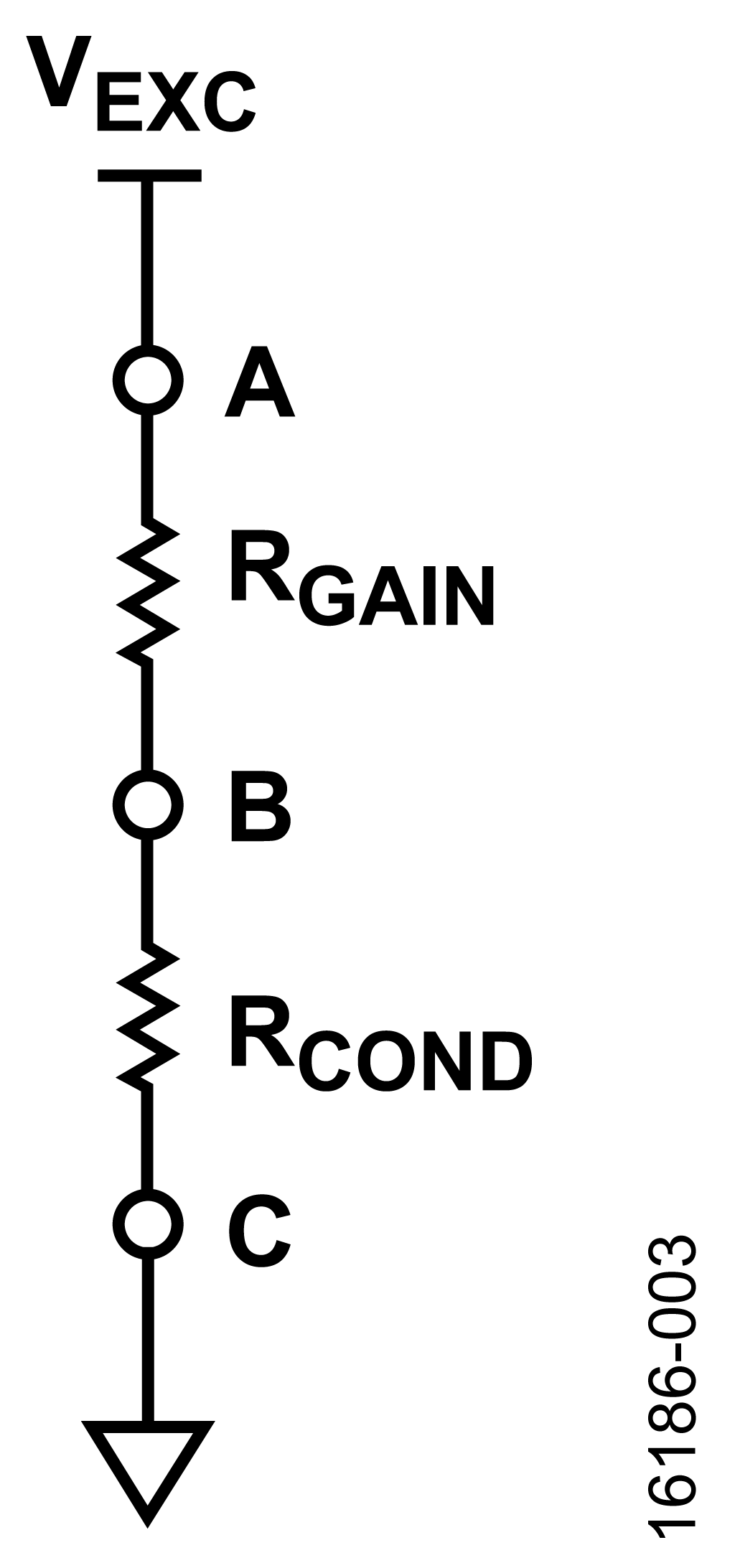
RGAIN sets the magnitude of the voltage across and current through the conductivity cell and solution simplified as RCOND. Node B and Node C are constantly switched to impose a bipolar square wave across RCOND. A multiplexer switches between different gain resistors in Node A. The applied excitation voltage at Node A to the voltage divider is generated using AD5683R, a 16-bit SPI voltage digital-to-analog converter (DAC). This allows the magnitude of the square wave signal applied to the voltage divider to be user-configurable. Choose the excitation voltage to maximize the signal while not exceeding the probe’s ratings. By default, the software applies 0.4 V excitation. The AD5683R is also by default the source of the system’s 2.5 V reference voltage, but can also be configured to accept an external reference voltage.

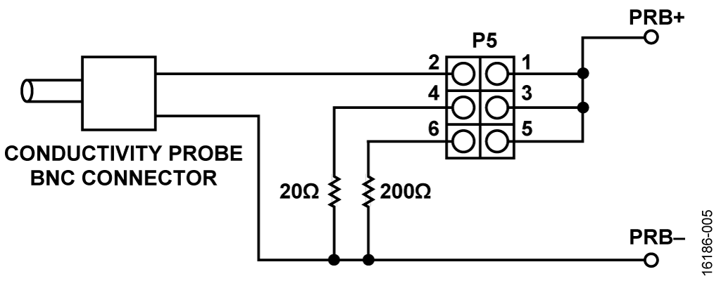
Figure 4 shows the gain setting resistors and switch, where R1 =20 Ω, R2 = 200 Ω, R3 = 2 kΩ, R4 = 20 kΩ, R5 = 200 kΩ, R6 =2 MΩ, R7 = 20 MΩ and P1, P2, and P3 are GPIO outputs fromthe AD7124-8. The circuit has a usable conductance range of 1 µS to 1 S. The voltage divider of the conductivity cell scales through these ranges by switching between seven gain resistors using ADG1608 as shown in Figure 4. The ADG1608 is an 8-channel multiplexer with a typical on-resistance of 12.5 Ω when operating at a single 5 V supply. This on-resistance is significant when the conductivity measurement is in the 20 to 200 Ω range. Pin S2 and Pin S3 of the ADG1608, which connect to the 20 Ω and 200 Ω gain resistors, respectively, are also connected to two input channels of the analog-to-digital converter (ADC). The system can also be configured to perform an initial calibration for measurement errors in the 20 and 200 Ω range. Shown in Figure 5 is a 3-option (6-pin) jumper selection header (P5), which connects to 20 Ω and 200 Ω precision resistors. Shorting Pin 1 and Pin 2 configures the system to measure the signal across the conductivity cell while shorting Pin 3 and Pin 4 or Pin 5 and Pin 6 configures the system to measure the signal across the precision resistors.
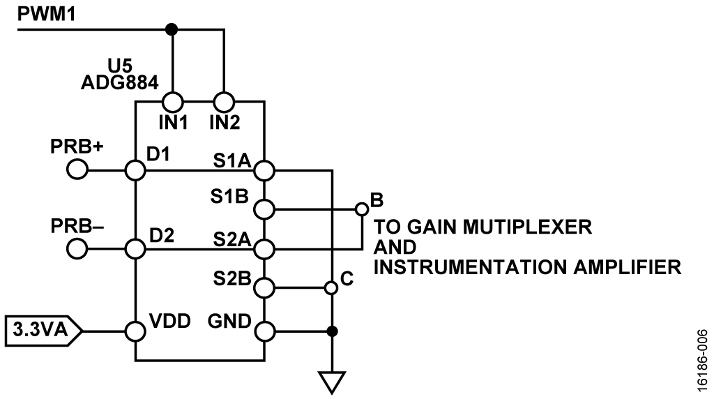
The conductivity cell is switched to impose a bipolar signal across it using an ADG884 as shown in Figure 6. The ADG884 has 0.5 Ω typical on-resistance and is operating at a single 3.3 V supply. The switching is controlled by a PWM signal from the microcontroller board. The frequency of this signal is userconfigurable to 94 Hz for low conductivity measurements and 2.4 kHz for high conductivity measurements.
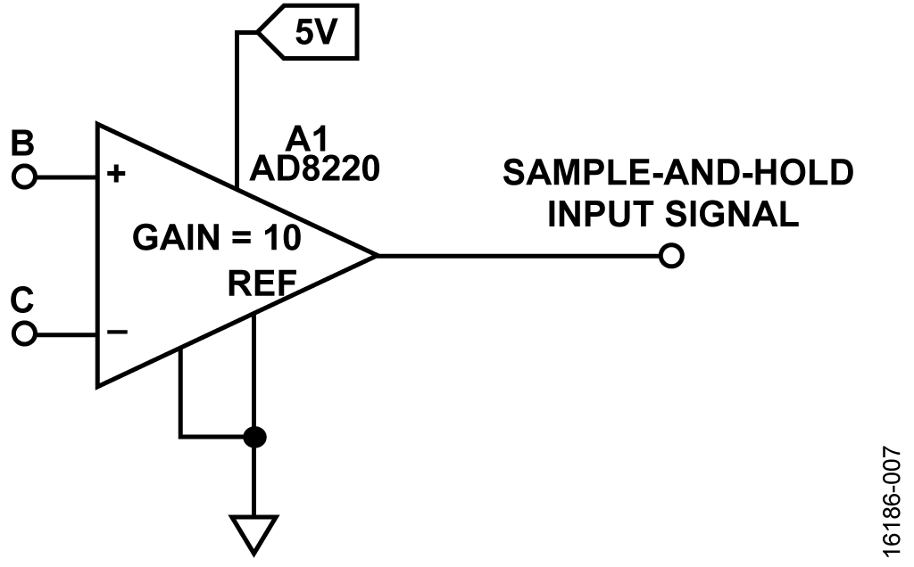
The signal across the conductivity cell is amplified by a gain of 10 using the AD8220 low input bias current instrumentation amplifier operating at a single 5 V supply with input signals up to 0.25 V as shown in Figure 7. There is also a user-configurable jumper selector P6, which provides for a system zero-scale calibration.
The output of the instrumentation amplifier passes through two parallel sample-and-hold circuits. As shown in Figure 8, the sampling of the AD8220 output is controlled by the ADG836, a dual SPDT switch, which has low charge-injection and is operating at a single 3.3 V supply with input signals of up to 2.5 V.
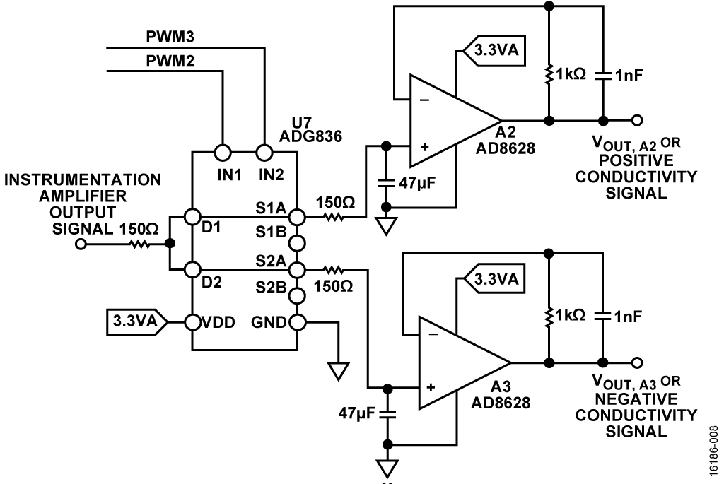
The switch connects the two parallel sample-and-hold circuitsusing PWM1 and PWM2 at the middle of the positive andnegative cycles of the main PWM1 signal. The switchingdiagram for the three PWM signals and the voltage across theconductivity cell is shown in Figure 9.

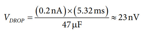
This sampling method decreases the electrode capacitance effects at the beginning of the PWM1 signal state change as well as the electrode polarization effects occurring at the end of each state. This causes the output of the sample-and-hold circuit to be two dc levels corresponding to ten times the positive and negative voltage values across the conductivity cell, respectively. The maximum charge injection due to the switching is 40 pC, which constitutes an error of 40 pC ÷ 47 µF ≈ 851 nV. The worst case drop voltage is the product of half the period of the low frequency switching and the droop rate, which is the worst-case leakage current of the ADG836 and the worst-case bias currents of the AD8628 divided by the hold capacitance. As shown in Equation 4, this drop voltage is theoretically 23 nV.
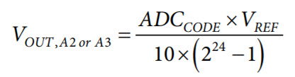
The outputs of A2 and A3 AD8628 buffer amplifier are applied to the single-ended ADC AD7124-8 input channels, AIN7 and AIN8, respectively. These input channels are referenced by default to the AD5683 reference voltage. AD7124-8 is userconfigurable to perform either single or continuous sampling. It is also user-configurable to perform a system zero-scale calibration using the selectable precision resistors in P5 or read the multiplexer on-resistance using the input channels from the 20 Ω and 200 Ω gain resistors. The positive and negative output voltages is computed from the 24-bit unipolar ADC code using Equation 5.
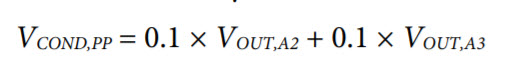
where: Equation 6 shows the calculation of the peak-to-peak voltage across the conductivity cell from the AD8628 output voltages.
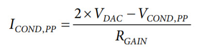
The current through the conductivity cell can be calculatedfrom the peak-to-peak cell voltage, gain resistance, andexcitation or DAC voltage using Equation 7.
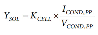
The conductivity YSOL of the solution is given by Equation 8.
where KCELL is the conductivity cell constant. Substituting Equation 7 and Equation 8 into Equation 9 yields the following equation:
Equation 9 shows that the conductivity measurement depends on the conductivity cell constant, the excitation voltage, the gain resistance used and the sum of the two voltage outputs of each sample-and-hold channel. Temperature CompensationConductivity measurements are also temperature dependent; conductance increases as temperature increases. Most commercial conductivity probes have an integrated RTD, facilitating temperature compensation. The typical method to compensate the conductivity measurement to a standard reference temperature is through a linear function dependent on the temperature coefficient α, which is based on the type of ions present in the solution as shown in Equation 10. Usually, the reference temperature is set at 25 ˚C.
where: YREF is the conductivity referenced to TREF. Y is the conductivity at temperature T. TREF is the reference temperature. T is the solution temperature. α is the temperature coefficient The typical values of α for common salt solutions are shown in Table 2.
The TDS of the solution in mg/L is calculated from the referenced conductivity measurement using Equation 11.
where ke is the TDS factor. The TDS factor is calculated by measuring the referenced conductivity of a standard known TDS solution as shown in Equation 12.
where: TDSREF,STD is the known TDS value of the solution at TREF. YREF,STD is the measured conductivity of the solution at TREF. The conductivity measurement cannot distinguish between constituents and individual types of ions. Thus, the TDS factor varies at a specific range, which is distinct for each type of solution. Table 3 shows the typical range of the TDS factors of common salt solutions.
Temperature MeasurementConductivity varies significantly with the temperature of the solution and the temperature coefficients are also significantly for each type of solution. A simple method of measuring the temperature of a solution uses a 2-wire RTD. The simplified front-end schematic is shown in Figure 10.
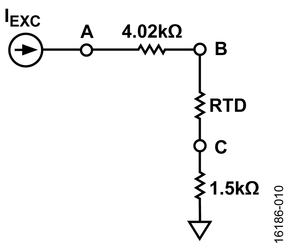
The AD7124-8 contains two matched software configurable constant current sources, which have eight selectable current output values and can be made available to any of the analog input channels. The excitation current to the RTD resistor network is set to 250 µA from the AIN0 channel. Node A and Node B are connected to the AD7124-8 external reference input. Node B and Node C, which constitute the differential RTD signal, are connected to the AD7124-8 analog input channels. Both differential inputs are passed through two identical and typical RC low-pass filter as shown in Figure 11.
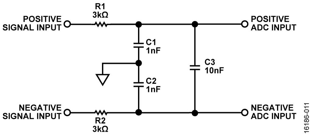
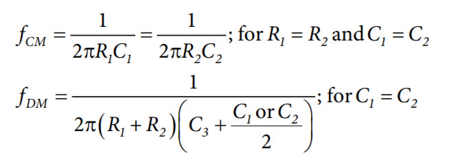
This low-pass filter topology provides attenuation of both differential and common-mode noise signals. The large value of R1 and R2 in Figure 11 also help to protect against 30 V miswiring.C1 and C2 are the common-mode capacitors and are set to a tenth of the differential-mode capacitor C3. This attenuates the effects of noise due to mismatch between the common-mode capacitors. The common mode cut-off frequency (fCM) is approximately 20 times the differential mode cut-off frequency (fDM), which are 53 kHz and 2.5 kHz, respectively. The calculations are shown in Equation 13.
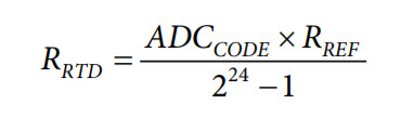
where: fCM is the common mode cut-off frequency. fDM is the differential mode cut-off frequency. All resistance values for the RTD are referenced or capped to 4.02 kΩ and the reference voltage is 250 µA × 4.02 kΩ = 1.005 V. Also, the system can accommodate both Pt100 or Pt1000 RTDs. The resistance of the RTD (RRTD) is computed from the 24-bit unipolar ADC code using Equation 14.
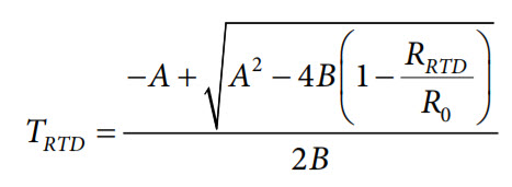
where: ADCCODE is the 24-bit unipolar code of the signal sample. RREF is the reference resistor. RREF = 4.02 kΩ. The Callender-Van Dusen equation is used to define the relation of the RTD resistance and temperature. For temperatures greater than or equal to 0˚C or for resistances greater than or equal to R0, the temperature in degrees Celsius can be computed using Equation 15, which can be obtained directly from the Callender-Van Dusen equation.
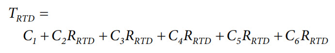
where: A = 3.9083 ×10⁻³ . B = −5.775 ×10⁻⁷ . C = −4.183 × 10⁻¹². R0 is the RTD resistance at 0˚C. RRTD is the RTD resistance at TRTD. TRTD is the temperature in degrees Celsius. For temperatures below 0˚C or for resistances below R0, a best fit polynomial expression is used as shown in Equation 16.
where: Software Operation Settings
The provided software configures six parameters for TDS
The DAC voltage can be set to any value from 0 to 2.5 V. At startup, the DAC voltage is set to 400 mV. The selected gain resistance can be set to open or any of the seven resistor values: 20 Ω, 200 Ω, 2 kΩ, 20 kΩ, 200 kΩ, 2 MΩ, and 20 MΩ. Initially, the gain resistance is set to open. The type of RTD used can be set to either Pt100 or Pt1000. Initially, the type of RTD used in temperature measurements is set to Pt100. The frequency of the PWM signal sets the frequency of thebipolar pulse across the conductivity cell. The software can onlyswitch between two options for PWM frequency: 94 Hz and2.4 kHz. Initially, the PWM frequency is set to 94 Hz. There are three fixed options for conductivity probe cellconstants: 0.1, 1.0, and 10. A forth option allows the user toenter a custom value for probes with cell constants other than0.1, 1.0, and 10. By default, the cell constant is set to 1.0. The type of solution sets the TDS factor and temperaturecoefficient used in computing for TDS and temperaturecompensation, respectively. The software has built-in settingsfor only sodium chloride (NaCl) and potassium chloride (KCl)solutions. However, the user can set custom values for the TDSfactor and temperature coefficient separately for other types ofsolutions. Initially, the type of solution is set to NaCl. Apart from these parameters, the software can also switchbetween taking measurements with the ADC in singleconversion mode and with the ADC in continuous conversionmode. In single conversion mode, the ADC goes to idle modewhenever a read conductivity command is not being issued.This decreases the power consumption of the board when it isnot active. Additionally, the DAC voltage value can be set tozero in these times to further decrease the board’s consumption.In continuous conversion mode, the ADC continuously samplesthe conductivity cell signal. This decreases the measurementtime for each sample, which makes this effective whencontinuously monitoring the conductivity of a solution.
Auto-Ranging Conductivity Measurement

Calibration Procedure
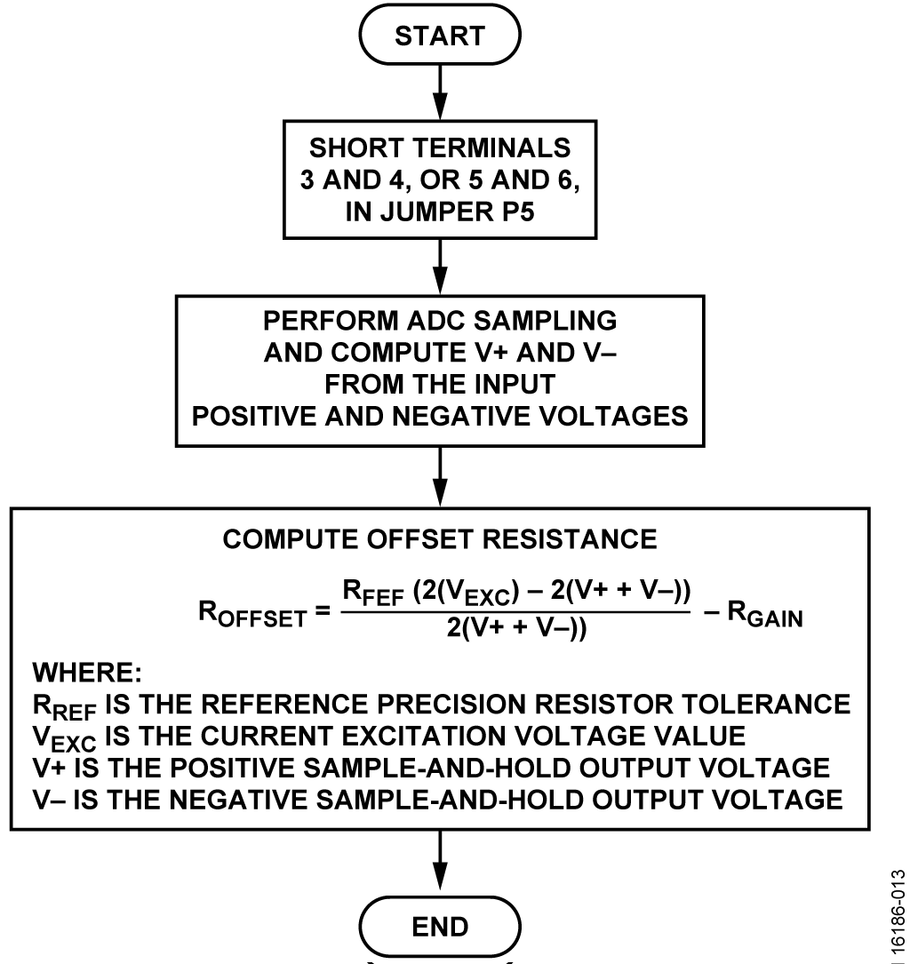
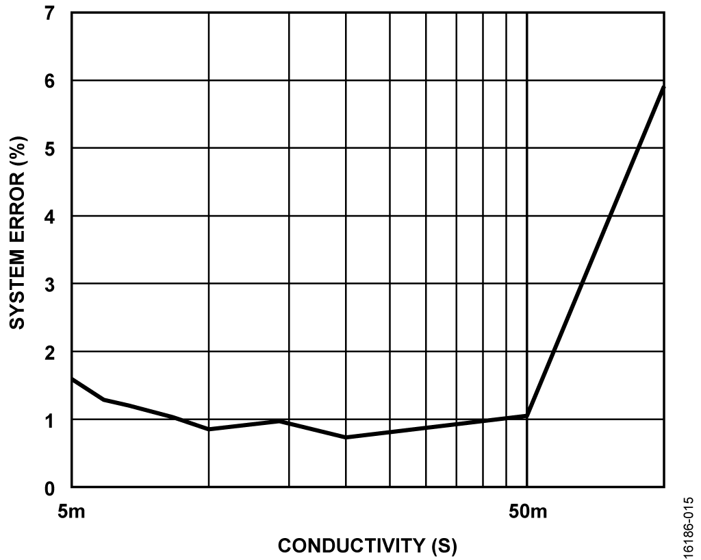
Both these two calibration methods need to be done only oncefor each board since the software stores the output of thecalibration procedures. System AccuracyFrom Equation 9, the computation of conductivity depends onthe two output voltages of the sample-and-hold topology, RGAIN,and the DAC output voltage. RGAIN resistors below the MΩrange have 0.1% tolerance while the 2 MΩ and 20 MΩ resistorshave 1% tolerance. Added to the resistances in the simplevoltage divider network shown in Figure 3 are the onresistancesof the multiplexer ADG1608 and the conductivitycell switch ADG884, which are maximum at 17.4 Ω and 0.96 Ω,respectively. The input bias currents and input offset currentfrom the instrumentation amplifier introduces a voltage, whichscales with the gain resistance and the resistance of the solution.The B-grade AD8220 has a max input bias current of 10 pA foreach input and a max input offset current of 0.6 pA, whichmakes a total input bias current of 20.6 pA. At 20 MΩ, thisconstitutes a 20.6 pA × 20 MΩ = 412 µV input bias voltage.Moreover, at a gain of 10, the AD8220 has a 0.2% max gainerror. Computing conductivity directly from a known precisionresistance measures the system accuracy and accounts for allthese factors, including the ones introduced by the sample-andholdtopology, such as the drop voltage in Equation 4. Figure 14 shows the measured accuracy of the conductivitymeasurements taken using precision resistors from 1 MΩ to10 Ω, corresponding to conductivities of 1 µS to 0.1 S. Anincrease in the system errors is visible in the 10 mS to 100 mSrange. For these ranges, a calibration method to on-boardprecision resistances (shown in Figure 5) is required.  Calibration is performed only once for each board and an offsetresistance is obtained, which accounts for the on-resistance ofthe multiplexer. The software system stores the offset resistancevalue and uses it for all succeeding conductivity measurementsuntil the calibration method is performed again. Figure 15shows the error for high conductivities when calibrated to the20 Ω precision resistance shown in Figure 5.
System Noise PerformanceAs shown in Figure 16, the noise level of the system is only15.99 nS for a 10 kΩ precision resistance corresponding to a100 µS conductance.

|


 热点图文
热点图文