NXP公司的i.MX 6UltraLite是高性能超高效率处理器系列,采用先进的单核ARM Cortex®-A,运行速度最高支持528 MHz,包括一个集成的电源管理模块,降低了外接电源的复杂性,简化了上电时序.器件提供多种存储器接口,其中包括LPDDR2,DDR3,DDR3L,NAND闪存,NOR 闪存,eMMC,Quad SPI等;i.MX 6UltraLite也提供各种接口用于连接外围设备,如WLAN,Bluetooth™,GPS,显示器和摄像头传感器.主要用在ePOS设备,IoT网关,门禁控制面板,人机接口(HMI)和智能家电.本文介绍了i.MX 6UltraLite主要特性,系统框图,以及评估板MCIMX6UL-EVK主要特性,框图,电路图和材料清单以及硬件设计文件.
i.MX6UL: i.MX 6UltraLite Processor - Low-power, secure, Arm® Cortex®-A7 Core The i.MX 6UltraLite is a high performance, ultraefficient processor family featuring NXP’s advancedimplementation of the single ARM Cortex®-A7 core,which operates at speeds up to 528 MHz. The i.MX6UltraLite includes an integrated power managementmodule that reduces the complexity of the externalpower supply and simplifies the power sequencing. Eachprocessor in this family provides various memoryinterfaces, including LPDDR2, DDR3, DDR3L, Rawand Managed NAND flash, NOR flash, eMMC, QuadSPI, and a wide range of other interfaces for connectingperipherals, such as WLAN, Bluetooth™, GPS,displays, and camera sensors.
The i.MX 6UltraLite is specifically useful forapplications such as:
• Electronics Point-of-Sale device
• Telematics
• IoT Gateway
• Access control panels
• Human Machine Interfaces (HMI)
• Smart appliances
The features of the i.MX 6UltraLite processor include1:
• Single-core ARM Cortex-A7―The single core A7 provides a cost-effective and power-efficientsolution.
• Multilevel memory system―The multilevel memory system of each device is based on the L1instruction and data caches, L2 cache, and internal and external memory. The device supportsmany types of external memory devices, including DDR3, low voltage DDR3, LPDDR2, NORFlash, NAND Flash (MLC and SLC), OneNAND™, Quad SPI, and managed NAND, includingeMMC up to rev 4.4/4.41/4.5.
• Smart speed technology―Power management implemented throughout the IC that enablesmultimedia features and peripherals to consume minimum power in both active and various lowpower modes.
• Dynamic voltage and frequency scaling―The processor improves the power efficiency by scalingthe voltage and frequency to optimize performance.
• Multimedia powerhouse―Multimedia performance is enhanced by a multilevel cache system,NEON™ MPE (Media Processor Engine) co-processor, a programmable smart DMA (SDMA)controller, an asynchronous audio sample rate converter, and a Pixel processing pipeline (PXP) tosupport 2D image processing, including color-space conversion, scaling, alpha-blending, androtation.
• Ethernet interfaces―10/100 Mbps Ethernet controllers.
• Human-machine interface―Support digital parallel display interface.
• Interface flexibility―Each processor supports connections to a variety of interfaces: High-speedUSB on-the-go with PHY, multiple expansion card port (high-speed MMC/SDIO host and other),12-bit ADC module, CAN port, smart card interface compatible with EMV Standard v4.3, and avariety of other popular interfaces (such as UART, I2C, and I2S serial audio).
• Advanced security―The processor delivers hardware-enabled security features that enable securee-commerce, digital rights management (DRM), information encryption, secure boot, and securesoftware downloads. The security features are discussed in detail in the i.MX 6UltraLite SecurityReference Manual (IMX6ULSRM).
• Integrated power management―The processor integrates linear regulators and internally generatevoltage levels for different domains. This significantly simplifies system power managementstructure.
i.MX 6UltraLite主要特性:
The i.MX 6UltraLite processors are based on ARM Cortex-A7 MPCore™ Platform, which has thefollowing features:
• Supports single ARM Cortex-A7 MPCore (with TrustZone) with:
― 32 KBytes L1 Instruction Cache
― 32 KBytes L1 Data Cache
― Private Timer
― Cortex-A7 NEON Media Processing Engine (MPE) Co-processor
• General Interrupt Controller (GIC) with 128 interrupts support
• Global Timer
• Snoop Control Unit (SCU)
• 128 KB unified I/D L2 cache (on G2 and G3 devices only)
• Single Master AXI bus interface output of L2 cache (for G2 and G3 devices only)
The SoC-level memory system consists of the following additional components:
― Boot ROM, including HAB (96 KB)
― Internal multimedia/shared, fast access RAM (OCRAM, 128 KB)
― Secure/non-secure RAM (32 KB)
• External memory interfaces: The i.MX 6UltraLite processors support handheld DRAM, NOR, andNAND Flash memory standards.
― 16-bit LP-DDR2-800, 16-bit DDR3-800 and LV-DDR3-800
― 8-bit NAND-Flash, including support for Raw MLC/SLC, 2 KB, 4 KB, and 8 KB page size,BA-NAND, PBA-NAND, LBA-NAND, OneNAND™, and others. BCH ECC up to 40 bits.
― 16/8-bit NOR Flash. All EIMv2 pins are muxed on other interfaces.
Each i.MX 6UltraLite processor enables the following interfaces to external devices (some of them aremuxed and not available simultaneously):
• Displays:
― One parallel display port supports max 85 MHz display clock and up to WXGA (1366 x 768)at 60 Hz
― Support 24-bit, 18-bit, 16-bit, and 8-bit parallel display
• Camera sensors1:
― One parallel camera port, up to 24 bit and 148.5 MHz pixel clock
― Support 24-bit, 16-bit, 10-bit, and 8-bit input
― Support BT.656 interface
• Expansion cards:
― Two MMC/SD/SDIO card ports all supporting:
C 1-bit or 4-bit transfer mode specifications for SD and SDIO cards up to UHS-I SDR-104
mode (104 MB/s max)
C 1-bit, 4-bit, or 8-bit transfer mode specifications for MMC cards up to 52 MHz in both SDRand DDR modes (104 MB/s max)
C 4-bit or 8-bit transfer mode specifications for eMMC chips up to 200 MHz in HS200 mode(200 MB/s max)
• USB:
― Two high speed (HS) USB 2.0 OTG (Up to 480 Mbps), with integrated HS USB Phy
• Miscellaneous IPs and interfaces:
― Three SAI supporting up to three I2S
― Sony Philips Digital Interconnect Format (SPDIF), Rx and Tx
― Eight UARTs, up to 5.0 Mbps each:
C Providing RS232 interface
C Supporting 9-bit RS485 multidrop mode
C Support RTS/CTS for hardware flow control
― Four enhanced CSPI (eCSPI)
― Four I2C
― Two 10/100 Ethernet Controller (IEEE1588 compliant)
― Eight Pulse Width Modulators (PWM)
― System JTAG Controller (SJC)
― GPIO with interrupt capabilities
― 8x8 Key Pad Port (KPP)
― One Quad SPI
― Two Flexible Controller Area Network (FlexCAN)
― Three Watchdog timers (WDOG)
― Two 12-bit Analog to Digital Converters (ADC) with up to 10 input channels in total
― Touch Screen Controller (TSC)
The i.MX 6UltraLite processors integrate advanced power management unit and controllers:
• Provide PMU, including LDO supplies, for on-chip resources
• Use Temperature Sensor for monitoring the die temperature
• Use Voltage Sensor for monitoring the die voltage
• Support DVFS techniques for low power modes
• Use SW State Retention and Power Gating for ARM and NEON
• Support various levels of system power modes
• Use flexible clock gating control scheme
• Two smart card interfaces compatible with EVM Standard 4.3
The i.MX 6UltraLite processors use dedicated hardware accelerators to meet the targeted multimediaperformance. The use of hardware accelerators is a key factor in obtaining high performance at low powerconsumption, while having the CPU core relatively free for performing other tasks.
The i.MX 6UltraLite processors incorporate the following hardware accelerators:
• PXP―Pixel Processing Pipeline for imagine resize, rotation, overlay, and CSC1. Off loading keypixel processing operations are required to support the LCD display applications.
• ASRC―Asynchronous Sample Rate Converter
Security functions are enabled and accelerated by the following hardware:
• ARM TrustZone including the TZ architecture (separation of interrupts, memory mapping, etc.)
• SJC―System JTAG Controller. Protecting JTAG from debug port attacks by regulating orblocking the access to the system debug features.
• CAAM―Cryptographic Acceleration and Assurance Module, containing cryptographic and hashengines, 32 KB secure RAM, and True and Pseudo Random Number Generator (NIST certified).
• SNVS―Secure Non-Volatile Storage, including Secure Real Time Clock.
• CSU―Central Security Unit. CSU is configured during boot and by eFUSEs and determine thesecurity level operation mode as well as the TZ policy.
• A-HAB―Advanced High Assurance Boot―HABv4 with the new embedded enhancements:SHA-256, 2048-bit RSA key, version control mechanism, warm boot, CSU, and TZ initialization.
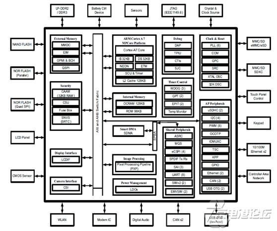
图1.i.MX 6UltraLite系统框图
i.MX 6UltraLite目标应用:
Consumer Electronics
Smart Connected Appliances
Networking
Smart Metering Connectivity
Secure Transaction and Retail Payments
Point of Sale (POS) Reader
评估板MCIMX6UL-EVK
This EVK board is a platform designed to showcase many ofthe most commonly used features of the i.MX 6UltraLiteApplications Processor in a small, low cost package. Thei.MX 6UltraLite EVK board is an entry level developmentboard, which gives the developer the option of becomingfamiliar with the processor before investing a large amountor resources in more specific designs.
评估板MCIMX6UL-EVK主要特性:
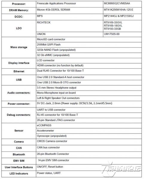
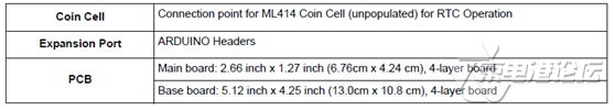
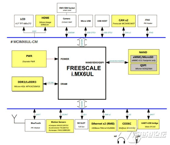
图2.评估板MCIMX6UL-EVK框图
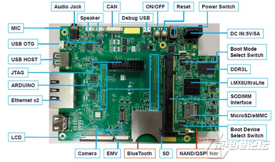
图3.评估板MCIMX6UL-EVK概述图
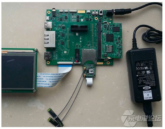
图4.评估板MCIMX6UL-EVK连接图
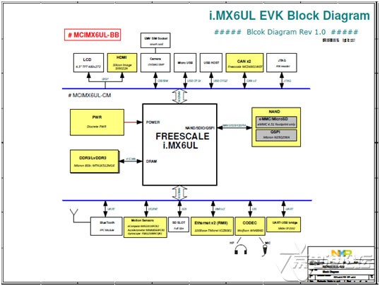
图5.评估板MCIMX6UL-EVK框图
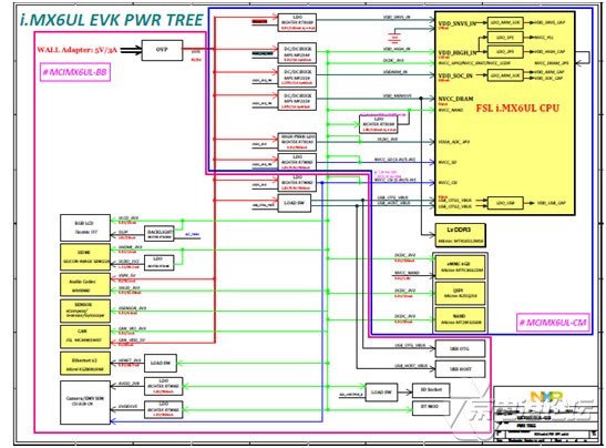
图6.评估板MCIMX6UL-EVK电路图(1)
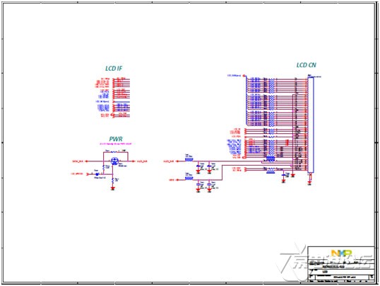
图7.评估板MCIMX6UL-EVK电路图(2)
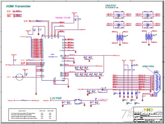
图8.评估板MCIMX6UL-EVK电路图(3)
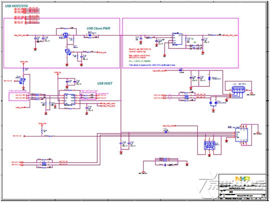
图9.评估板MCIMX6UL-EVK电路图(4)
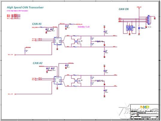
图10.评估板MCIMX6UL-EVK电路图(5)
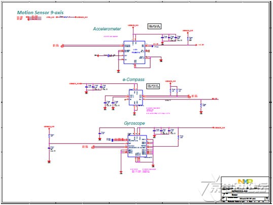
图11.评估板MCIMX6UL-EVK电路图(6)
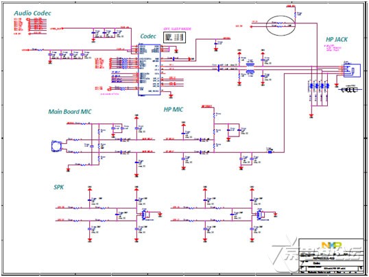
图12.评估板MCIMX6UL-EVK电路图(7)
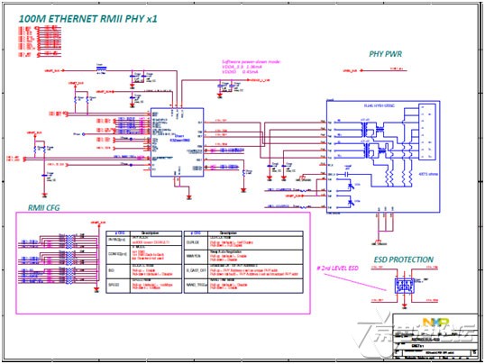
图13.评估板MCIMX6UL-EVK电路图(8)
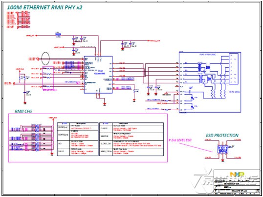
图14.评估板MCIMX6UL-EVK电路图(9)
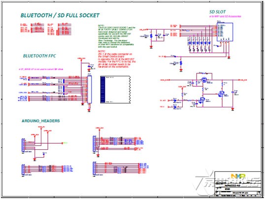
图15.评估板MCIMX6UL-EVK电路图(10)
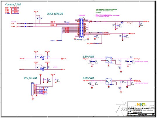
图16.评估板MCIMX6UL-EVK电路图(11)

图17.评估板MCIMX6UL-EVK电路图(12)
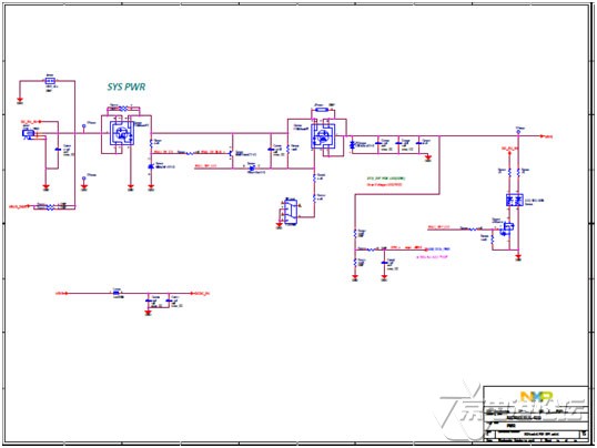
图18.评估板MCIMX6UL-EVK电路图(13)
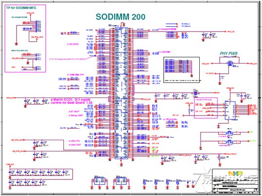
图19.评估板MCIMX6UL-EVK电路图(14)
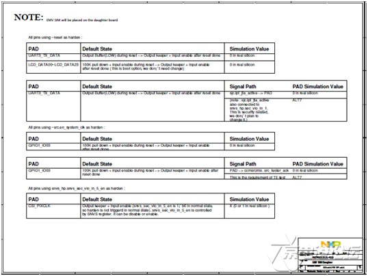
图20.评估板MCIMX6UL-EVK电路图(15)
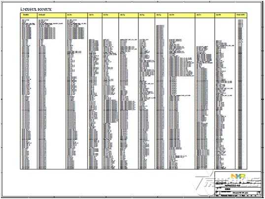
图21.评估板MCIMX6UL-EVK电路图(16)
评估板MCIMX6UL-EVK材料清单见:
 评估板MCIMX6UL-EVK材料清单.xls
详情请见:
http://www.nxp.com/docs/zh/data-sheet/IMX6ULCEC.pdf
和http://www.nxp.com/docs/en/user-guide/IMX6ULEVKHUG.pdf
 IMX6ULCEC.pdf
IMX6ULEVKHUG.pdf


 热点图文
热点图文