ST公司的STM32L4R9I是高性能超低功耗MCU系列产品,基于Arm® Cortex®-M4 32位RISC核,工作频率高达120MHz,支持所有ARM单精度数据处理指令和所有数据类型,并能实现全套的DSP指令和存储器保护单元(MPU),使得应用更加安全.电源电压1.7V-3.6V,关断模式33 nA,工作温度-40℃ 到 85/125℃,主要用在健康手环,智能手表,小型医疗设备,智能表计和智能工业传感器等各种产品的中央控制器.本文介绍了STM32L4R9I主要特性,框图和时钟树,以及评估板STM32L4R9I-EVAL主要特性,框图,电路图,材料清单和PCB主要元件分布图.
The STM32L4R5xx, STM32L4R7xx and STM32L4R9xx devices are an ultra-low-power microcontrollers family (STM32L4+ Series) based on the high-performance Arm® Cortex®-M4 32-bit RISC core. They operate at a frequency of up to 120 MHz.
The Cortex-M4 core features a single-precision floating-point unit (FPU), which supports all the Arm® single-precision data-processing instructions and all the data types. The Cortex-M4 core also implements a full set of DSP (digital signal processing) instructions and a memory protection unit (MPU) which enhances the application’s security.
These devices embed high-speed memories (2 Mbytes of Flash memory and 640 Kbytes of SRAM), a flexible external memory controller (FSMC) for static memories (for devices with packages of 100 pins and more), two OctoSPI Flash memories interface (available on all packages) and an extensive range of enhanced I/Os and peripherals connected to two APB buses, two AHB buses and a 32-bit multi-AHB bus matrix.
The STM32L4Rxxx devices embed several protection mechanisms for embedded Flash memory and SRAM: readout protection, write protection, proprietary code readout protection and a firewall.
These devices offer a fast 12-bit ADC (5 Msps), two comparators, two operational amplifiers, two DAC channels, an internal voltage reference buffer, a low-power RTC, two general-purpose 32-bit timer, two 16-bit PWM timers dedicated to motor control, seven general-purpose 16-bit timers, and two 16-bit low-power timers. The devices support four digital filters for external sigma delta modulators (DFSDM). In addition, up to 24 capacitive sensing channels are available. They also feature standard and advanced communication interfaces such as:
• Four I2Cs
• Three SPIs
• Three USARTs, two UARTs and one low-power UART
• Two SAIs
• One SDMMC
• One CAN
• One USB OTG full-speed
• Camera interface
• DMA2D controller
The devices operate in the -40 to +85℃ (+105 ℃ junction) and -40 to +125℃ (+130 ℃ junction) temperature ranges from a 1.71 to 3.6 V for VDD power supply when using internal LDO regulator and a 1.05 to 1.32 V VDD12 power supply when using external SMPS supply. A comprehensive set of power-saving modes allows the design of low-power applications.
Some independent power supplies are supported like an analog independent supply input for ADC, DAC, OPAMPs and comparators, a 3.3 V dedicated supply input for USB and up to 14 I/Os, which can be supplied independently down to 1.08 V. A VBAT input allows to backup the RTC and backup the registers. Dedicated VDD12 power supplies can be used to bypass the internal LDO regulator when connected to an external SMPS.The STM32L4Rxxx family offers six packages from 100-pin to 169-pin.
STM32L4R9I主要特性:
• Ultra-low-power with FlexPowerControl
C 1.71 V to 3.6 V power supply
C -40 ℃ to 85/125 ℃ temperature range
C Batch acquisition mode (BAM)
C 305 nA in VBAT mode: supply for RTC and 32x32-bit backup registers
C 33 nA Shutdown mode (5 wakeup pins)
C 125 nA Standby mode (5 wakeup pins)
C 420 nA Standby mode with RTC
C 2.8 μA Stop 2 with RTC
C 110 μA/MHz Run mode (LDO mode)
C 43 μA/MHz Run mode (@ 3.3 V SMPS mode)
C 5 μs wakeup from Stop mode
C Brownout reset (BOR) in all modes except shutdown
C Interconnect matrix
• Core: Arm® 32-bit Cortex®-M4 CPU with FPU, adaptive real-time accelerator (ART Accelerator™) allowing 0-wait-state execution from Flash memory,frequency up to 120 MHz, MPU, 150 DMIPS/1.25 DMIPS/MHz (Dhrystone 2.1), and DSP instructions
• Performance benckmark
C 1.25 DMIPS/MHz (Drystone 2.1)
C 410.32 Coremark® (3.42 Coremark/MHz @120 MHz)
• Energy benckmark
C 233 ULPMark™CP score
C 54.7 ULPMark™PPscore
• Clock sources
C 4 to 48 MHz crystal oscillator
C 32 kHz crystal oscillator for RTC (LSE)
C Internal 16 MHz factory-trimmed RC (±1%)
C Internal low-power 32 kHz RC (±5%)
C Internal multispeed 100 kHz to 48 MHz oscillator, auto-trimmed by LSE (better than ±0.25 % accuracy)
C Internal 48 MHz with clock recovery
C 3 PLLs for system clock, USB, audio, ADC
• RTC with HW calendar, alarms and calibration
• Up to 24 capacitive sensing channels: support touchkey, linear and rotary touch sensors
• Advanced graphics features
C Chrom-ART Accelerator™ (DMA2D) for enhanced graphic content creation
C Chrom-GRC™ (GFXMMU) allowing up to 20% of graphic resources optimization
C MIPI® DSI Host controller with two DSI lanes running at up to 500 Mbits/s each
C LCD-TFT controller
• 16x timers: 2 x 16-bit advanced motor-control, 2 x 32-bit and 5 x 16-bit general purpose, 2x 16-bit basic, 2x low-power 16-bit timers (available in Stop mode), 2x watchdogs, SysTick timer
• Up to 136 fast I/Os, most 5 V-tolerant, up to 14 I/Os with independent supply down to 1.08 V
• Memories
C 2-Mbyte Flash, 2 banks read-while-write, proprietary code readout protection
C 640 Kbytes of SRAM including 64 Kbytes with hardware parity check
C External memory interface for static memories supporting SRAM, PSRAM, NOR, NAND and FRAM memories
C 2 x OctoSPI memory interface
• 4x digital filters for sigma delta modulator
• Rich analog peripherals (independent supply)
C 12-bit ADC 5 Msps, up to 16-bit with hardware oversampling, 200 μA/Msps
C 2x 12-bit DAC, low-power sample and hold
C 2x operational amplifiers with built-in PGA
C 2x ultra-low-power comparators
• 20x communication interfaces
C USB OTG 2.0 full-speed, LPM and BCD
C 2x SAIs (serial audio interface)
C 4x I2C FM+(1 Mbit/s), SMBus/PMBus
C 6x USARTs (ISO 7816, LIN, IrDA, modem)
C 3x SPIs (5x SPIs with the dual OctoSPI)
C CAN (2.0B Active) and SDMMC
• 14-channel DMA controller
• True random number generator
• CRC calculation unit, 96-bit unique ID
• 8- to 14-bit camera interface up to 32 MHz (black&white) or 10 MHz (color)
• Development support: serial wire debug (SWD), JTAG, Embedded Trace Macrocell (ETM)
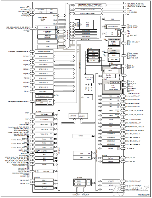
图1.STM32L4R5xx, STM32L4R7xx和STM32L4R9xx框图
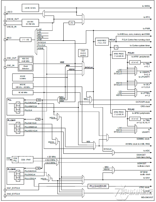
图2. STM32L4R5xx, STM32L4R7xx和STM32L4R9xx时钟树
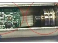
STM32L4R9AI MCU评估板STM32L4R9I-EVAL
The STM32L4R9I-EVAL evaluation board is designed as a complete demonstration and development platform for STMicroelectronics’Arm® Cortex®-M4 core-based STM32L4R9AI microcontroller with: four I²C buses, three SPI and six USART ports, CAN port, two SAI ports, 12-bit ADC, 12-bit DAC, internal 640-Kbyte SRAM and 2-Mbyte Flash memory, two Octo-SPI memory interfaces, touch-sensing capability, USB OTG FS port,LCD-TFT controller, MIPI DSI host controller, flexible memory controller (FMC), 8- to 14-bit camera interface, and JTAG debugging support.
The full range of on-board hardware features helps the user to evaluate all the peripherals (USB, USART, digital microphones, ADC and DAC, TFT LCD, MIPI DSI LCD, LDR, SRAM, NOR Flash memory device, Octo-SPI Flash memory device, microSD card, sigma-delta modulators, CAN transceiver, EEPROM) and to develop applications. Extension headers allow easy connection of a daughterboard or wrapping board for a specific application.An ST-LINK/V2-1 is integrated on the board, as an embedded in-circuit debugger and programmer for the STM32 MCU and the USB virtual COM port bridge.
评估板STM32L4R9I-EVAL主要特性:
• STM32L4R9AII6 Arm-based microcontroller with 2 Mbytes of Flash memory and 640 Kbytes of RAM in a UFBGA169 package
• 1.2” 390x390 pixels MIPI DSI round LCD
• 4.3” 480x272 pixels TFT LCD with RGB mode
• Two ST-MEMS digital microphones
• 8-Gbyte microSD card bundled
• 16-Mbit (1 M x 16 bit) SRAM device
• 128-Mbit (8 M x 16 bit) NOR Flash memory device
• 512-Mbit Octo-SPI Flash memory device with double transfer rate (DTR) support
• 64-Mbit Octo-SPI SRAM memory device with HyperBus interface support
• EEPROM supporting 1 MHz I²C-bus communication speed
• Reset and wake-up / tamper buttons
• Joystick with four-way controller and selector
• Touch-sensing button
• Light-dependent resistor (LDR)
• Potentiometer
• Coin battery cell for power backup
• Board connectors:
C Two jack outputs for stereo audio headphone with independent content
C Slot for microSD card supporting SD and SDHC
C TFT LCD standard connector
C MIPI DSI display standard connector
C EXT_I2C connector supports I²C bus
C RS-232 port configurable for communication or MCU flashing
C USB OTG FS Micro-AB port
C CAN 2.0A/B-compliant port
C Connector for ADC input and DAC output
C JTAG/SWD connector
C ETM trace debug connector
C User interface through USB virtual COM port
C Embedded ST-LINK/V2-1 debug and flashing facility
C TAG connector
C STDC14 connector
C PMOD connector
• Board expansion connectors:
C Motor-control connector
C Extension connector for daughterboard
• Flexible power-supply options: power jack, ST-LINK/V2-1 USB connector, USB OTG FS connector, daughterboard
• On-board ST-LINK/V2-1 debugger/programmer with USB re-enumeration capability:
mass storage, virtual COM port and debug port
• Microcontroller supply voltage: fixed 3.3 V or adjustable range from 1.71 V to 3.6 V
• MCU current consumption measurement circuit
• Access to comparator and operational amplifier of STM32L4R9AII6
• Comprehensive free software libraries and examples available with the STM32Cube package
• Support of a wide choice of integrated development environments (IDEs) including IAR™, Keil®, GCC-based IDEs
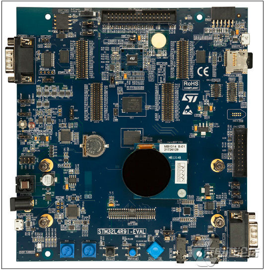
图3.评估板STM32L4R9I-EVAL(顶视)和DSI显示MB1314子板外形图
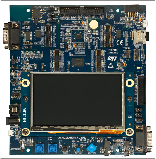
图4.评估板STM32L4R9I-EVAL(顶视)和TFT LCD MB1315子板外形图
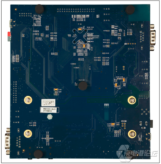
图5.评估板STM32L4R9I-EVAL(底视)外形图
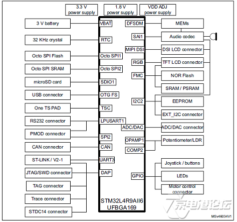
图6.评估板STM32L4R9I-EVAL框图
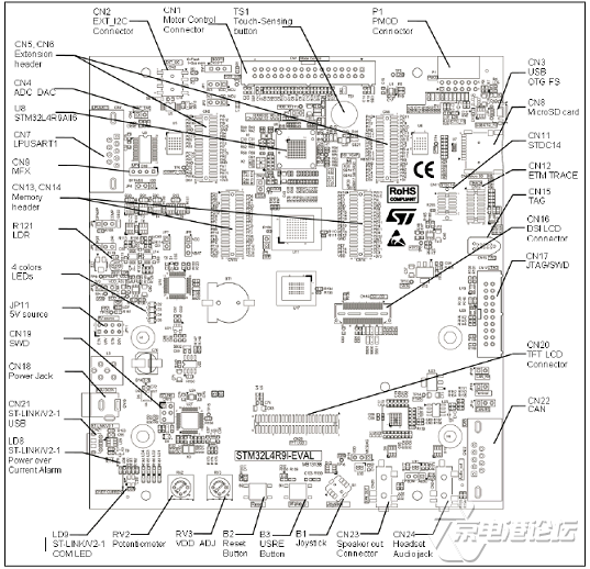
图7.评估板STM32L4R9I-EVAL顶层元件分布图
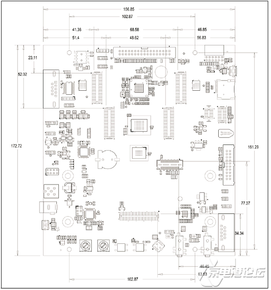
图8.评估板MB1313 STM32L4R9I-EVAL元件分布图
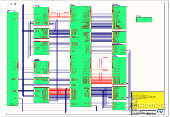
图9.评估板STM32L4R9I-EVAL电路图(1)
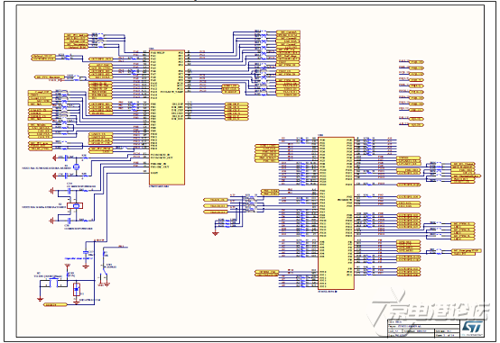
图10.评估板STM32L4R9I-EVAL电路图(2):MCU
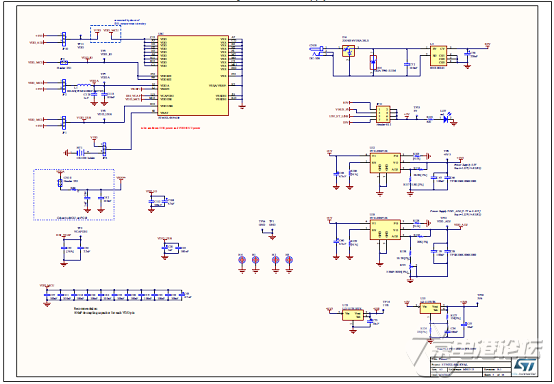
图11.评估板STM32L4R9I-EVAL电路图(3):电源
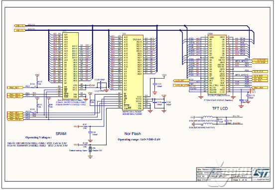
图12.评估板STM32L4R9I-EVAL电路图(4):SRAM和NOR闪memorv器件和TFT LCD
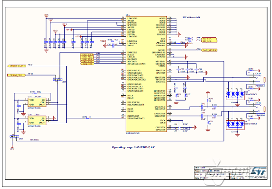
图13.评估板STM32L4R9I-EVAL电路图(5):音频CODEC
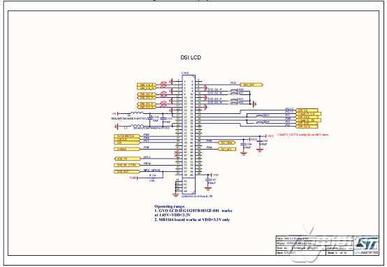
图14.评估板STM32L4R9I-EVAL电路图(6):DSI显示器连接器
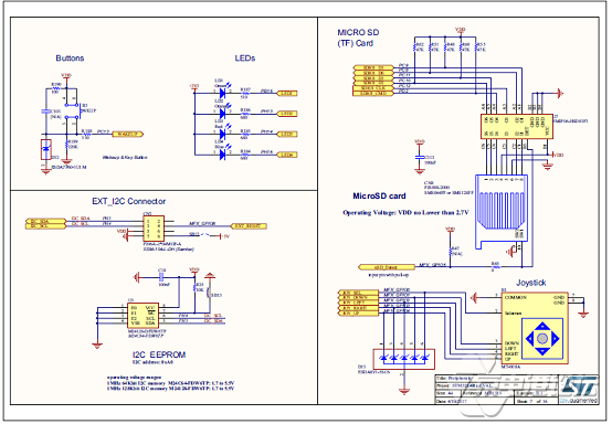
图15.评估板STM32L4R9I-EVAL电路图(7):物理控制外设,microSD和EEPROM
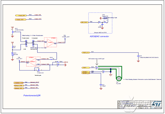
图16.评估板STM32L4R9I-EVAL电路图(8):模拟输入和输出与触摸检测器件
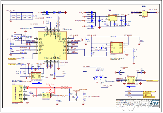
图17.评估板STM32L4R9I-EVAL电路图(9):ST-LINK/V2-1
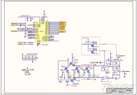
图18.评估板STM32L4R9I-EVAL电路图(10):IDD测量

图19.评估板STM32L4R9I-EVAL电路图(11):JTAG和跟踪调试连接器
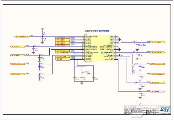
图20.评估板STM32L4R9I-EVAL电路图(12):马达控制器连接器
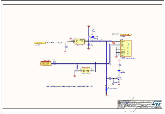
图21.评估板STM32L4R9I-EVAL电路图(13):USB OTG端口

图22.评估板STM32L4R9I-EVAL电路图(14):USART,CAN收发器和PMOD连接器
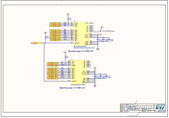
图23.评估板STM32L4R9I-EVAL电路图(15):Octo-SPI闪存
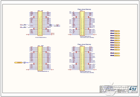
图24.评估板STM32L4R9I-EVAL电路图(16):扩展连接器
评估板STM32L4R9I-EVAL材料清单见:
详情请见:
http://www.st.com/content/ccc/resource/technical/document/datasheet/group3/98/80
/dc/e5/f8/4b/4b/a3/DM00366448/files/DM00366448.pdf/jcr:content/translations/en.DM00366448.pdf


 热点图文
热点图文