|
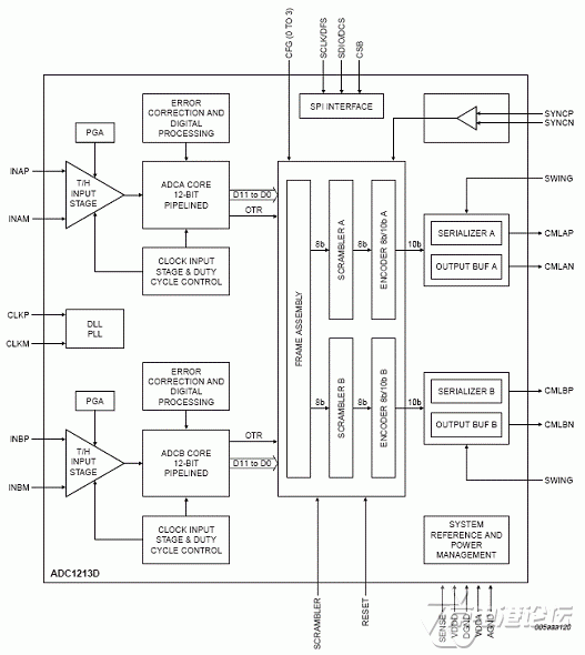
nxp 公司的ADC1213D系列是双路取样频率从65Msps到125Msps的12位模数转换器,具有宽动态范围和低功耗特点,流水线架构和输出误差修正包管ADC1213D系列在整个工作范围内不会丢码.单电源工作:模拟电源3.3 V,输出驱动器1.8 V.ADC1213D的SNR达73dB,SFDR为90dBc.可用在有线和无线宽带通信,频谱分析,手提仪表,超声设备和图像设备.本文先容了ADC1213D系列主要特点,方框架图,输入取样电路,单个和两个变压器配置图, 基准等效电路图以及所实现的JESD240A串行器详细框架图. ADC1213D065/080/105/125:Dual 12-bit ADC; 65, 80, 105 or 125 Msps The ADC1213D is a dual channel 12-bit Analog-to-Digital Converter (ADC) optimized for high dynamic performances and low power at sample rates up to 125 Msps. Pipelined architecture and output error correction ensure the ADC1213D is accurate enough to guarantee zero missing codes over the entire operating range. Supplied from a 3.3 V source for analog and a 1.8 V source for the output driver, it can output data in serial mode, because of the two lanes of differential outputs, which are compliant with the JESD204A standard. An integrated Serial Peripheral Interface (SPI) allows the user to easily configure the ADC. A set of IC configurations is also available via the binary level control pins, which are used at power-up. The device also includes a programmable gain amplifier with flexible input voltage range. Excellent dynamic performance is maintained from the baseband to input frequencies of 170 MHz or more, making the ADC1213D ideal for use in communications, imaging and medicine. ADC1213D主要特点: SNR,73 dB SFDR,90 dBc Sample rate up to 125 Msps Dual channel 12-bit pipelined ADC core 3.3V, 1.8V single supplies Flexible input voltage range: 1V(p-p)to 2V(p-p)with 6 dB programmable fine gain Offset binary, 2’s complement, gray code 2 configurable serial outputs Compliant with JESD204A serial transmission standard HVQFN56 package INL 1 LSB; DNL0.5 LSB Input bandwidth, 600 MHz Power dissipation, 995 mW at 80 Msps Duty cycle stabilizer High IF capability Power-down and Sleep modes ADC1213D应用: Wireless and wired broadband communications Spectral analysis Portable instrumentation Ultrasound equipment Imaging systems 详情请复制打开此衔接地址: |


 热点图文
热点图文