Renesas公司的RX65N是接纳32位RXv2 CPU核的高性能mcu,最大工作频率120MHz,在120MHz时的性能240DMIOS,单精度32位IEEE-754浮点,嵌入了90nm和40nm快速存储器,在核处理,代码效率和功耗上具有极好的性能,片上还集成了混淆信号外设,工作电压2.7到3.6-V,主要用在物联网毗连和马达控制等.本文先容了RX65N主要特点,框架图,以及RX65N入门开辟板(RSK)主要特点和指标,框架图,元件结构图,电路图和质料清单.
RX65N, RX651 group are highly compatible among the same series both in functional scalability and pin assignments.
In addition, driver/middleware (FIT support) and sample code-generation tools (code generators) and evaluation boards (starter kits) to allow reuse of most of developed hardware/software resources, enabling seamless and scalable product development from small to large scale applications without effort in a short-time.
RX65N主要特点:
■ 32-bit RXv2 CPU core
Max. operating frequency: 120 MHz
Capable of 240 DMIPS in operation at 120 MHz
Single precision 32-bit IEEE-754 floating point
Two types of multiply-and-accumulation unit (between memoriesand between registers)
32-bit multiplier (fastest instruction execution takes one CPU clockcycle)
Divider (fastest instruction execution takes two CPU clock cycles)
Fast interrupt
CISC Harvard architecture with 5-stage pipeline
Variable-length instructions: Ultra-compact code
Supports the memory protection unit (MPU)
JTAG and FINE (one-line) debugging interfaces
■ Low-power design and architecture
Operation from a single 2.7- to 3.6-V supply
Low power consumption: A product that supports all peripheralfunctions draws only 0.19 mA/MHz (Typ.).
RTC is capable of operation from a dedicated power supply.
Four low-power modes
■ On-chip code flash memory
Supports versions with up to 1 Mbytes of ROM
No wait cycles at up to 50 MHz or when the ROM cache is hit, onewaitstate at up to 100 MHz, two-wait state at above 100 MHz
User code is programmable by on-board or off-board programming.
■ On-chip SRAM
256 Kbytes of SRAM (no wait cycles)
8 Kbytes of standby RAM (backup on deep software standby)
■ Data transfer
DMACAa: 8 channels
DTCb: 1 channel
EXDMAC: 2 channels
DMAC for the Ethernet controller: 1 channel
■ Reset and supply management
Power-on reset (POR)
Low voltage detection (LVD) with voltage settings
■ Clock functions
External crystal oscillator or internal PLL for operation at 8 to 24MHz
Internal 240-kHz LOCO and HOCO selectable from 16, 18, and 20MHz
120-kHz clock for the IWDTa
■ Real-time clock
Adjustment functions (30 seconds, leap year, and error)
Real-time clock counting and binary counting modes are selectable
Time capture function(for capturing times in response to event-signal input)
■ Independent watchdog timer
120-kHz (1/2 LOCO frequency) clock operation
■ Useful functions for IEC60730 compliance
Oscillation-stoppage detection, frequency measurement, CRCA,IWDTa, self-diagnostic function for the A/D converter, etc.
Register write protection function can protect values in importantregisters against overwriting.
■ Various communications interfaces
Ethernet MAC (1 channel)
PHY layer (1 channel) for host/function or OTG controller(1 channel) with full-speed USB 2.0 transfer
CAN (compliant with ISO11898-1), incorporating 32 mailboxes(up to 2 channels)
SCIg and SCIh with multiple functionalities (up to 11 channels)
Choose from among asynchronous mode, clock-synchronous mode,smart-card interface mode, simplified SPI, simplified I2C, andextended serial mode.
SCIi with 16-byte transmission and reception FIFOs(up to 2 channels)
I2C bus interface for transfer at up to 1 Mbps (up to 2 channels)
Four-wire QSPI (1 channel) in addition to RSPIc (3 channels)
Parallel data capture unit (PDC) for the CMOS camera interface(not in 100-pin products)
SD host interface (optional: 1 channel) with a 1- or 4-bit SD bus foruse with SD memory or SDIO
SD slave interface (optional: 1 channel) with a 1- or 4-bit SD bus foruse with SD host interface
MMCIF with 1-, 4-, or 8-bit transfer bus width
■ External address space
Buses for full-speed data transfer (max. operating frequency of 60MHz)
8 CS areas
8-, or 16-bit bus space is selectable per area
Independent SDRAM area (128 Mbytes)
■ Up to 25 extended-function timers
16-bit TPUa, and MTU3a
8-bit TMRa (4 channels), 16-bit CMT (4 channels), 32-bit CMTW(2 channels)
■ 12-bit A/D converter
Two 12-bit units (8 channels for unit 0; 21 channels for unit 1)
Self diagnosis
Detection of analog input disconnection
■ 12-bit D/A converter: 2 channels
■ Temperature sensor for measuring temperaturewithin the chip
■ Encryption (optional)
AES (key lengths: 128, 192, and 256 bits)
■ Up to 111 pins for general I/O ports
5-V tolerance, open drain, input pull-up, switchable driving ability
■ Operating temp. range
C40C to +85C
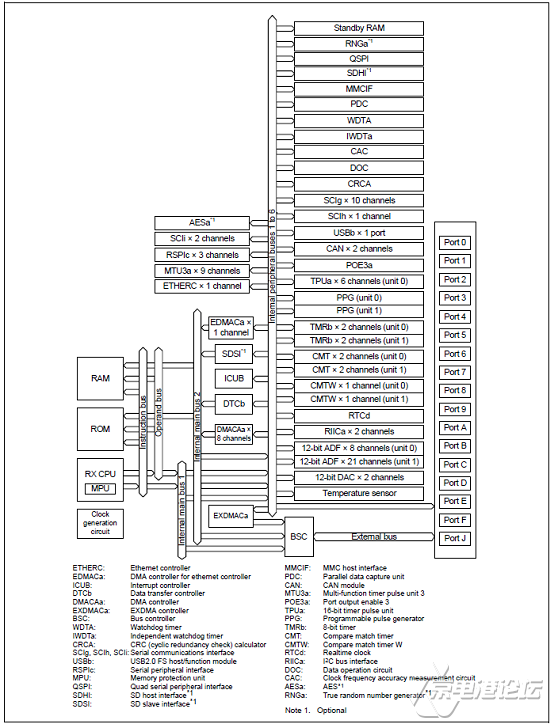
图1.RX65N框架图
RX65N入门开辟板(RSK)
The Renesas Starter Kit+ for RX65N is the perfect starter kit for developers who are new to the RX65N.
The kit includes an LCD display module, on-chip debugging emulator, and integrated development environment so you can start evaluating the RX65N immediately after opening the box.

图2.RX65N入门开辟板(RSK)外形图
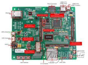
图3.RX65N入门开辟板(RSK)主要元件分布图
RX65N入门开辟板(RSK)主要特点:
1 channel Ethernet can be evaluated.
Mounts SD slot.
1 channel USB Function and 1 channel USB Host can be evaluated.
In addition, CAN, RSPI, QSPI, etc. can be evaluated.
Including sample codes(Sample programs will be available in Renesas Web site.) . Easy to understand coding technique.
RX65N入门开辟板(RSK)主要指标:
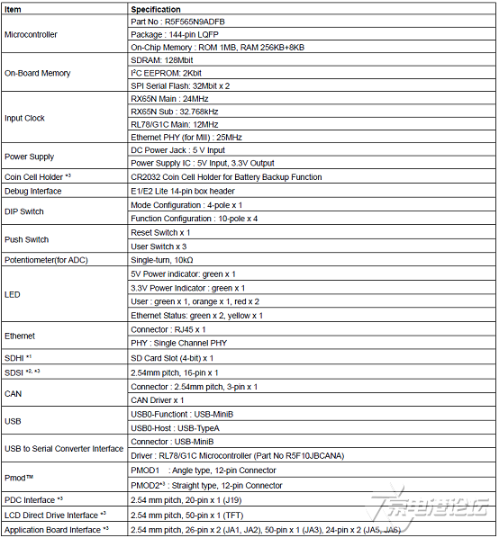
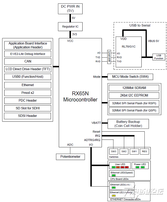
图4.RX65N入门开辟板(RSK)内部框架图

图5.RX65N入门开辟板(RSK)元件结构图
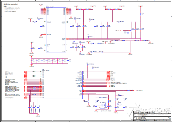
图6.RX65N入门开辟板(RSK)CPU板电路图(1)
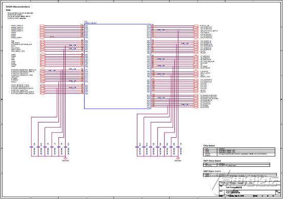
图7.RX65N入门开辟板(RSK)CPU板电路图(2)
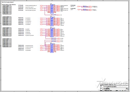
图8.RX65N入门开辟板(RSK)CPU板电路图(3)
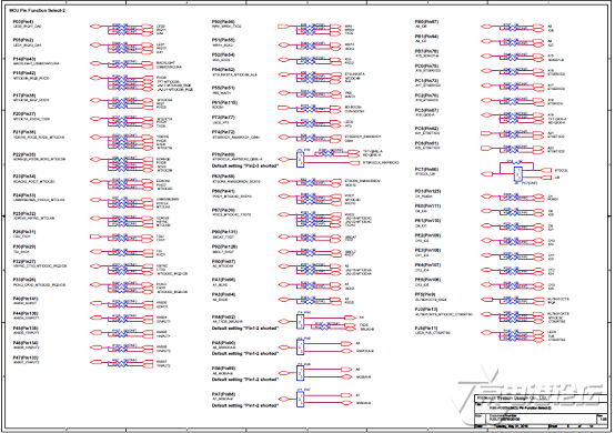
图9.RX65N入门开辟板(RSK)CPU板电路图(4)
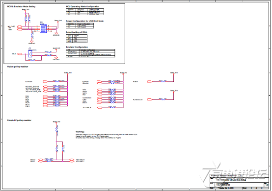
图10.RX65N入门开辟板(RSK)CPU板电路图(5)
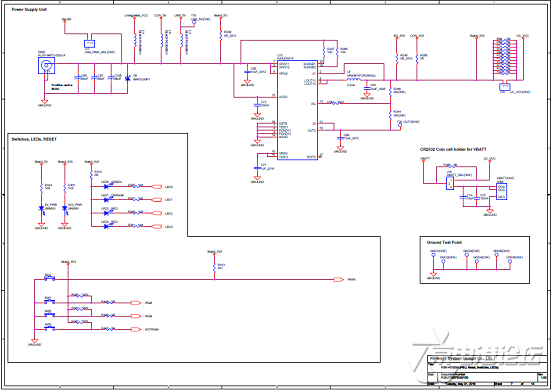
图11.RX65N入门开辟板(RSK)CPU板电路图(6)
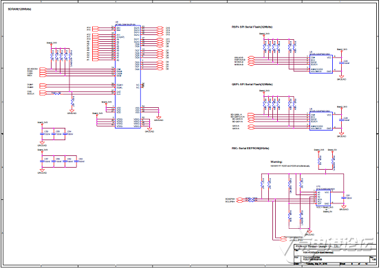
图12.RX65N入门开辟板(RSK)CPU板电路图(7)
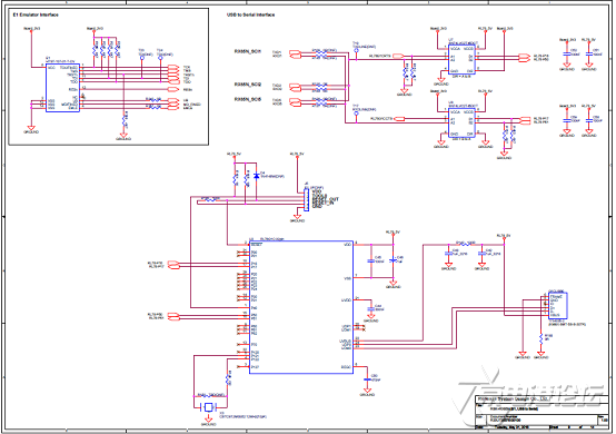
图13.RX65N入门开辟板(RSK)CPU板电路图(8)
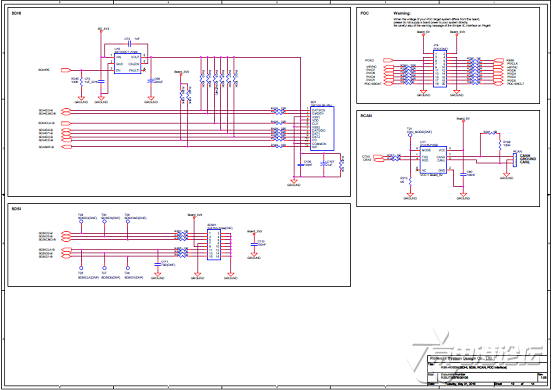
图14.RX65N入门开辟板(RSK)CPU板电路图(9)
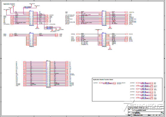
图15.RX65N入门开辟板(RSK)CPU板电路图(10)
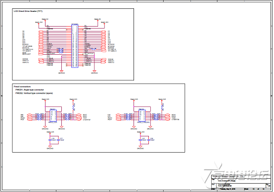
图16.RX65N入门开辟板(RSK)CPU板电路图(11)
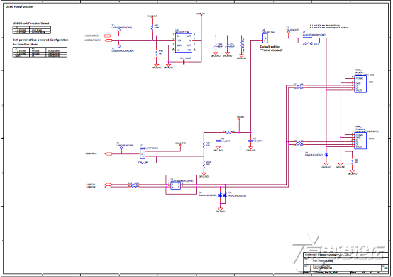
图17.RX65N入门开辟板(RSK)CPU板电路图(12)
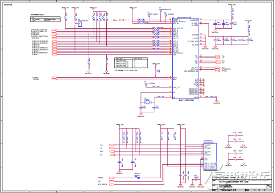
图18.RX65N入门开辟板(RSK)CPU板电路图(13)
RX65N入门开辟板(RSK)CPU板质料清单见:
 RSK+RX65N_BoM_Rev.1.00.xls
详情请复制打开此衔接地址:
http://www.renesas.com/en-us/docs/products/microcontrollers-microprocessors/rx/rx600/RX600_700_16page_brochure_120916_Final.pdf
和http://www.renesas.com/en-us/doc/products/mpumcu/doc/rx_family/r20ut3558eg0100-rsk+rx65n-usermanual.pdf
以及http://www.renesas.com/en-us/doc/products/mpumcu/doc/rx_family/r20ut3557eg0100-rsk+rx65n-schema.pdf
 r20ut3557eg0100-rsk+rx65n-schema.pdf
r20ut3558eg0100-rsk+rx65n-usermanual.pdf
RX600_700_16page_brochure_120916_Final.pdf


 热点图文
热点图文