|
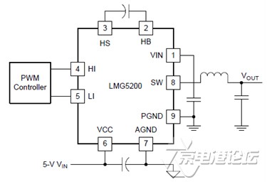
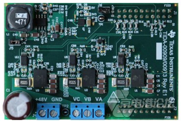
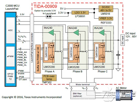
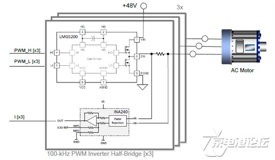
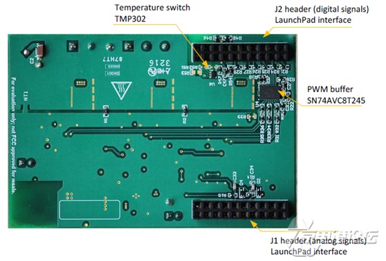
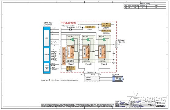
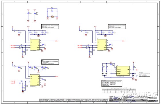
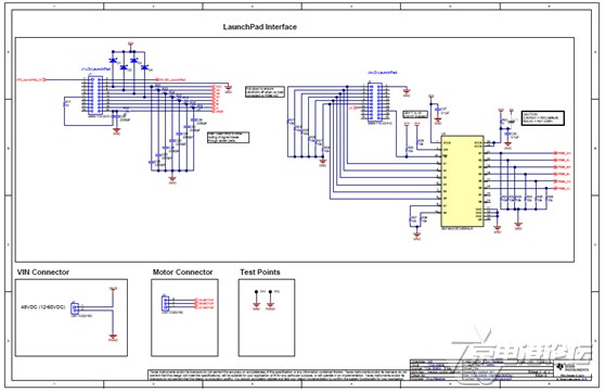
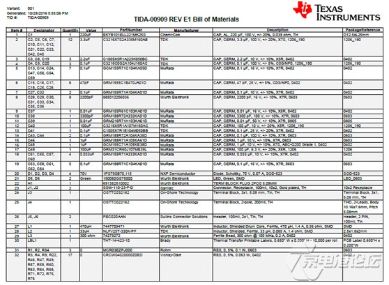
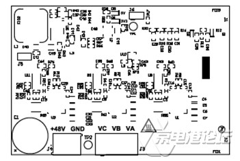
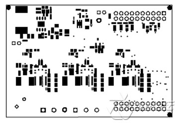
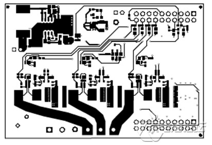
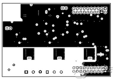
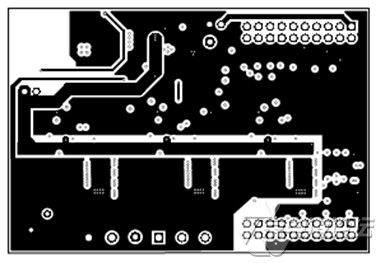
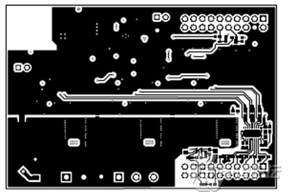
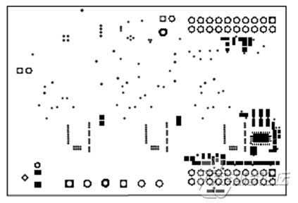
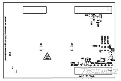
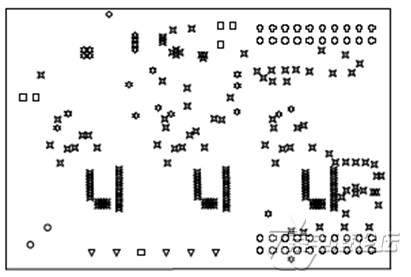
TI公司的LMG5200是80V GaN半桥功率级,包罗两个80V18-mΩGaN FET,输入电压高达80VDC,单独的高边和低边TTL输入,TTL逻辑输入能耐电压高达14V,时延典范为29.5ns,传输时延匹配2ns,主要用在CNC驱动,非军用无人机,电源转换,伺服驱动和马达控制.本文先容了LMG5200主要特点,功能框架图,48V/10A高频PWM三相GaN逆变器参考方案TIDA-00909主要特点,框架图,电路图,质料清单和PCB完整设计原理图. The LMG5200 device, a 80-V driver, GaN half-bridge power stage, provides an integrated power stage solution using enhancement-mode Gallium Nitride (GaN) FETs. The device consists of two, 80-V GaN FETs driven by one high-frequency GaN FET driver in a half-bridge configuration. The TTL logic compatible inputs can withstand input voltages up to 14 V regardless of the VCC voltage. The proprietary bootstrap voltage clamping technique ensures the gate voltages of the enhancement mode GaN FETs are within a safe operating range. GaN FETs provide significant advantages for power conversion as they have near zero reverse recovery and very small input capacitance CISS. All the devices are mounted on a completely bond-wire-free package platform with minimized package parasitic elements. The LMG5200 device is available in a 6 mm × 8 mm × 2 mm lead free package and can be easily mounted on PCBs. The device extends advantages of discrete GaN FETs by offering a more user-friendly interface. It is an ideal solution for applications requiring high-frequency, high-efficiency operation in a small form factor. It reduces the board requirements for maintaining clearance and creepage requirements for medium voltage GaN applications while minimizing the loop inductances to ensure fast switching. The LMG5200 device brings ease of designing high power density boards without the need for underfill whilemaintaining creepage and clearance requirements. The propagation delays between the high-side gate driverand low-side gate driver are matched to allow very tight control of dead time. Controlling the dead time is criticalin GaN-based applications to maintain high efficiency. HI and LI can be independently controlled to minimize thethird quadrant conduction of the low-side FET for hard switched buck converters. A very small propagationmismatch between the HI and LI to the drivers for both the falling and rising thresholds ensures dead times of<10 ns. Co-packaging the GaN FET half-bridge with the driver ensures minimized common source inductance. This minimized inductance has a significant performance impact on hard-switched topologies.The built in bootstrap circuit with clamp prevents the high-side gate drive from exceeding the GaN FETsmaximum gate-to-source voltage (Vgs) without any additional external circuitry. The built-in driver has anundervoltage lockout (UVLO) on the VDD and bootstrap (HB-HS) rails. When the voltage is below the UVLOthreshold voltage, the device ignores both the HI and LI signals to prevent the GaN FETs from being partially turned on. Below UVLO, if there is sufficient voltage (VVCC > 2.5 V), the driver actively pulls the high-side andlow-side gate driver output low. The UVLO threshold hysteresis of 200 mV prevents chattering and unwantedturn-on due to voltage spikes. Use an external VCC bypass capacitor with a value of 0.1 μF or higher. A size of0402 is recommended to minimize trace length to the pin. Place the bypass and bootstrap capacitors as close to the device as possible to minimize parasitic inductance. LMG5200主要特点: Input Voltage up to 80-V DC LMG5200应用: CNC Drives 48V/10A高频PWM三相GaN逆变器参考方案TIDA-00909 Low voltage, high-speed drives and/or low inductancebrushless motors require higher inverter switchingfrequencies in the range of 40 kHz to 100 kHz tominimize losses and torque ripple in the motor. TheTIDA-00909 reference design achieves this by usinga 3-phase inverter with three 80V/10A half-bridgeGaN power modules LMG5200 and uses shunt basedphase current sensing. Gallium nitride (GaN)transistors can switch much faster than silicon FETsand integrating the GaN FET and driver in the samepackage reduces parasitic inductances and optimizesswitching performance reducing losses, thus allowingto down-size or eliminate the heatsink. The TIDA-00909 offers a TI BoosterPack compatible interface toconnect to a C2000 MCU LaunchPad™ developmentkit for easy performance evaluation 三相GaN逆变器参考方案TIDA-00909特点: 3-phase GaN inverter with wide input voltagerange 12V to 60V and 7Arms/10Apeak outputcurrent, tested up to 100 kHz PWM. 三相GaN逆变器参考方案TIDA-00909应用: Servo Drives & Motion Control |


 lmg5200.pdf


 热点图文
热点图文