Microsemi公司的SmartFusion2 SoC FPGA系列集了第四代基于闪存的FPGA架构,ARM Cortex-M3处理器和高性能通信接口,是业界最低功耗最可靠和最安全简直可编逻辑办理方案.和以前的基于闪存的FPGA系列相比,提供3.6X门密度和2X性能;并包罗多个存储器区块和用于DSP处理的乘法累加区块.主要用在马达,工业自动化和高速I/O应用等.本文先容了SmartFusion2 SoC FPGA系列产物主要特点,框架图,系列产物表和SmartFusion2 高级开辟板M2S150-ADV-DEV-KIT主要特点,主要元件表,框架图,电路图,PCB元件结构图和质料清单.
Microsemi SmartFusion®2 SoC FPGAs integrate fourth generation flash-based FPGA fabric, an ARM Cortex-M3 processor, andhigh-performance communications interfaces on a single chip. The SmartFusion2 family is the industry’s lowest power, most reliableand highest security programmable logic solution. SmartFusion2 FPGAs offer up to 3.6X the gate density, up to 2X the performanceof previous flash-based FPGA families, and includes multiple memory blocks and multiply accumulate blocks for DSP processing.
The 166 MHz ARM Cortex-M3 processor is enhanced with an embedded trace macrocell (ETM), memory protection unit (MPU),8 Kbyte instruction cache, and additional peripherals, including controller area network (CAN), Gigabit Ethernet, and high speed universal serial bus (USB). High speed serial interfaces include PCI EXPRESS (PCIe), 10 Gbps attachment unit interface (XAUI) /XGMII extended sublayer (XGXS) plus native serialization/deserialization (SERDES) communication, while DDR2/DDR3 memory
controllers provide high speed memory interfaces.
SmartFusion2 SoC FPGA主要特点:
Reliability
• Single Event Upset (SEU) Immune
C Zero FIT FPGA Configuration Cells
• Junction Temperature: 125℃ C Military Temperature,100℃ C Industrial Temperature, 85℃ C CommercialTemperature, 125℃ - Automotive
• Single Error Correct Double Error Detect (SECDED)Protection on the Following:
C Ethernet Buffers
C CAN Message Buffers
C Cortex-M3 Embedded Scratch Pad Memory(eSRAMs)
C USB Buffers
C PCIe Buffer
C DDR Memory Controllers with Optional SECDEDModes
• Buffers Implemented with SEU Resistant Latches on theFollowing:
C DDR Bridges (MSS, MDDR, FDDR)
C Instruction Cache
C MMUART FIFOs
C SPI FIFOs
• NVM Integrity Check at Power-Up and On-Demand
• No External Configuration Memory Required―Instant-On, Retains Configuration When Powered Off
Security
• Design Security Features (Available on all Devices)
C Intellectual Property (IP) Protection Through UniqueSecurity Features and Use Models New to the PLDIndustry
C Encrypted User Key and Bitstream Loading,Enabling Programming in Less-Trusted Locations
C Supply-Chain Assurance Device Certificate
C Enhanced Anti-Tamper Features
C Zeroization
• Data Security Features
C Non-Deterministic Random Bit Generator (NRBG)
C User Cryptographic Services (AES-256, SHA-256,Elliptical Curve Cryptographic (ECC) Engine)
C User Physically Unclonable Function (PUF) KeyEnrollment and Regeneration
C CRI Pass-Through DPA Patent Portfolio License
C Hardware Firewalls Protecting MicrocontrollerSubsystem (MSS) Memories
Low Power
• Low Static and Dynamic Power
C Flash*Freeze Mode for Fabric
• Power as low as 13 mW/Gbps per lane for SERDESdevices
• Up to 50% lower total power than competing SoCdevices
High Performance FPGA
• Efficient 4-Input LUTs with Carry Chains for High-Performance and Low Power
• Up to 236 Blocks of Dual-Port 18 Kbit SRAM (LargeSRAM) with 400 MHz Synchronous Performance (512 x36, 512 x 32, 1 kbit x 18, 1 kbit x 16, 2 kbit x 9, 2 kbit x 8,4 kbit x 4, 8 kbit x 2, or 16 kbit x 1)
• Up to 240 Blocks of Three-Port 1 Kbit SRAM with 2Read Ports and 1 Write Port (micro SRAM)
• High-Performance DSP Signal Processing
C Up to 240 Fast Mathblocks with 18 x 18 SignedMultiplication, 17 x 17 Unsigned Multiplication and44-Bit Accumulator
Microcontroller Subsystem (MSS)
• Hard 166 MHz 32-Bit ARM Cortex-M3 Processor
C 1.25 DMIPS/MHz
C 8 Kbyte Instruction Cache
C Embedded Trace Macrocell (ETM)
C Memory Protection Unit (MPU)
C Single Cycle Multiplication, Hardware Divide
C JTAG Debug (4 wires), Serial Wire Debug (SWD,2 wires), and Serial Wire Viewer (SWV) Interfaces
• 64 KB Embedded SRAM (eSRAM)
• Up to 512 KB Embedded Nonvolatile Memory (eNVM)
• Triple Speed Ethernet (TSE) 10/100/1000 Mbps MAC
• USB 2.0 High Speed On-The-Go (OTG) Controller withULPI Interface
• CAN Controller, 2.0B Compliant, Conforms to
ISO11898-1, 32 Transmit and 32 Receive Buffers
• Two Each: SPI, I2C, Multi-Mode UARTs (MMUART)Peripherals
• Hardware Based Watchdog Timer
• 1 General Purpose 64-Bit (or two 32-bit) Timer(s)
• Real-Time Calendar/Counter (RTC)
• DDR Bridge (4 Port Data R/W Buffering Bridge to DDRMemory) with 64-Bit AXI Interface
• Non-Blocking, Multi-Layer AHB Bus Matrix AllowingMulti-Master Scheme Supporting 10 Masters and 7Slaves
• Two AHB-Lite/APB3 Interfaces to FPGA Fabric(Master/Slave Capable)
• Two DMA Controllers to Offload Data Transactions fromthe Cortex-M3 Processor
C 8-Channel Peripheral DMA (PDMA) for DataTransfer Between MSS Peripherals and Memory
C High-Performance DMA (HPDMA) for Data TransferBetween eSRAM and DDR Memories
Clocking Resources
• Clock Sources
C Up to Two High Precision 32 KHz to 20 MHz MainCrystal Oscillator
C 1 MHz Embedded RC Oscillator
C 50 MHz Embedded RC Oscillator
• Up to 8 Clock Conditioning Circuits (CCCs) with Up to 8Integrated Analog PLLs
C Output Clock with 8 Output Phases and 45° PhaseDifference (Multiply/Divide, and Delay Capabilities)
C Frequency: Input 1 MHz to 200 MHz, Output 20 MHzto 400 MHz
High Speed Serial Interfaces
• Up to 16 SERDES Lanes, Each Supporting:
C XGXS/XAUI Extension (To Implement a 10 Gbps(XGMII) Ethernet PHY Interface)
C Native SERDES Interface Facilitates Implementationof Serial RapidIO in Fabric or an SGMII Interface tothe Ethernet MAC in MSS
C PCI Express (PCIe) Endpoint Controllerx1, x2, x4 Lane PCI Express Core
Up to 2 Kbytes Maximum Payload Size
64-Bit/32-Bit AXI and 64-Bit/32-Bit AHB Masterand Slave Interfaces to the Application Layer
High Speed Memory Interfaces
• Up to 2 High Speed DDRx Memory Controllers
C MSS DDR (MDDR) and Fabric DDR (FDDR)Controllers
C Supports LPDDR/DDR2/DDR3
C Maximum 333 MHz DDR Clock Rate
C SECDED enable/Disable Feature
C Supports Various DRAM Bus Width Modes, x8, x9,x16, x18, x32, x36
C Supports Command Reordering to Optimize MemoryEfficiency
C Supports Data Reordering, Returning Critical WordFirst for Each Command
• SDRAM Support through the SMC_FIC and AdditionalSoft SDRAM Memory Controller
Operating Voltage and I/Os
• 1.2 V Core Voltage
• Multi-Standard User I/Os (MSIO/MSIOD)
C LVTTL/LVCMOS 3.3 V (MSIO Only)
C LVCMOS 1.2 V, 1.5 V, 1.8 V, 2.5 V
C DDR (SSTL2_1, SSTL2_2)
C LVDS, MLVDS, Mini-LVDS, RSDS DifferentialStandards
C PCI
C LVPECL (receiver only)
• DDR I/Os (DDRIO)
C DDR2, DDR3, LPDDR, SSTL2, SSTL18, HSTL
C LVCMOS 1.2 V, 1.5 V, 1.8 V, 2.5 V
• Market Leading Number of User I/Os with 5G SERDES

图1. SmartFusion2 SoC FPGA框架图
SmartFusion2 SoC FPGA系列产物表:

SmartFusion2 Advanced Development Kit(M2S150-ADV-DEV-KIT)
The SmartFusion®2 system-on-chip (SoC) field programmable gate array (FPGA) Advanced Development Kit(M2S150-ADV-DEV-KIT) is RoHS compliant and enables you to develop applications that involve the following:
• Microprocessor applications
• Embedded ARM® Cortex®-M3 processor based systems
• Motor control
• Industrial automation
• High speed I/O applications
• Universal serial bus (USB) applications (OTG support)contents of the SmartFusion2 Advanced Development Kit
M2S150-ADV-DEV-KIT包罗:
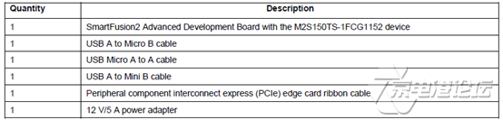
The M2S150-ADV-DEV-KIT device offers a full-featured 150 K logic element (LE) SmartFusion2 SoC FPGA. This150 K LE device has the following integrated on a single chip:
• Reliable flash-based FPGA fabric
• A 166 MHz Cortex-M3 processor
• Advanced security processing accelerators
• Digital signal processing (DSP) blocks
• Static random-access memory (SRAM)
• embedded nonvolatile memory (eNVM)
• High-performance communication interfaces
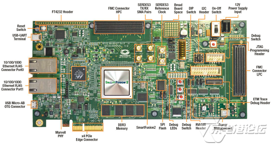
图2. SmartFusion2 SoC高级开辟板M2S150-ADV-DEV-KIT外形图
SmartFusion2高级开辟板M2S150-ADV-DEV-KIT主要元件表:

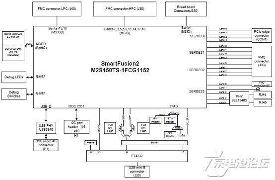
图3. SmartFusion2 SoC高级开辟板框架图
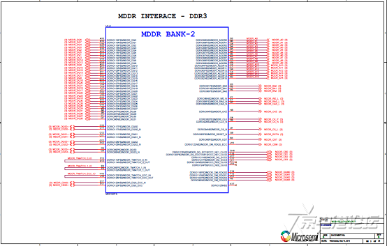
图4. SmartFusion2 SoC高级开辟板电路图(1)

图5. SmartFusion2 SoC高级开辟板电路图(2)
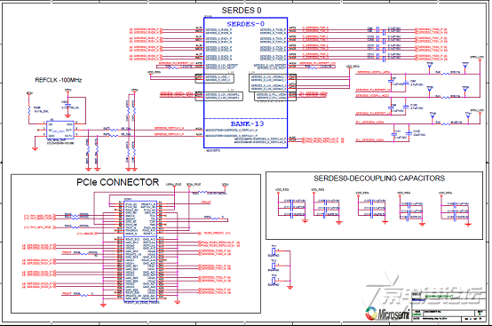
图4. SmartFusion2 SoC高级开辟板电路图(1)

图5. SmartFusion2 SoC高级开辟板电路图(2)
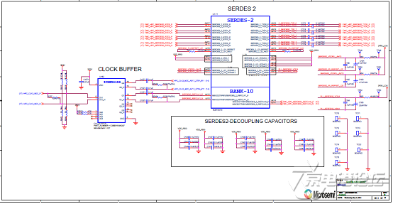
图6. SmartFusion2 SoC高级开辟板电路图(3)
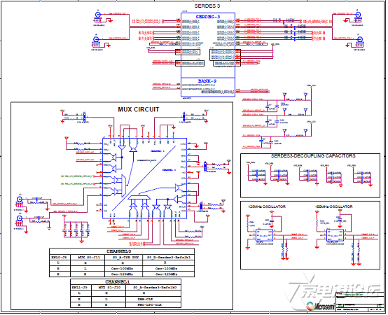
图7. SmartFusion2 SoC高级开辟板电路图(4)
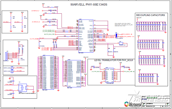
图8. SmartFusion2 SoC高级开辟板电路图(5)

图9. SmartFusion2 SoC高级开辟板电路图(6)

图10. SmartFusion2 SoC高级开辟板电路图(7)
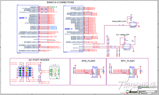
图11. SmartFusion2 SoC高级开辟板电路图(8)
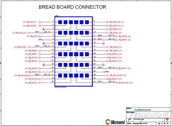
图12. SmartFusion2 SoC高级开辟板电路图(9)

图13. SmartFusion2 SoC高级开辟板电路图(10)

图14. SmartFusion2 SoC高级开辟板电路图(11)
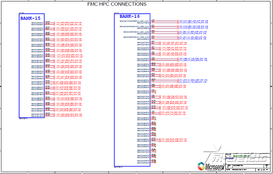
图15. SmartFusion2 SoC高级开辟板电路图(12)
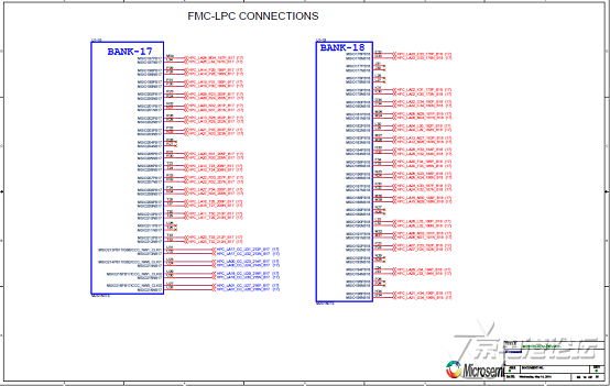
图16. SmartFusion2 SoC高级开辟板电路图(13)
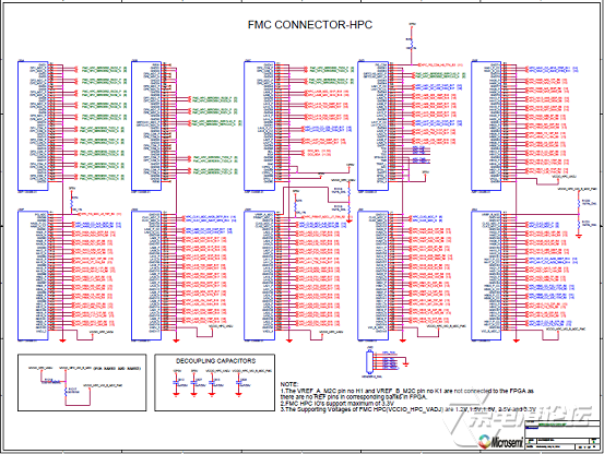
图17. SmartFusion2 SoC高级开辟板电路图(14)

图18. SmartFusion2 SoC高级开辟板电路图(15)
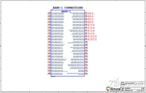
图19. SmartFusion2 SoC高级开辟板电路图(16)
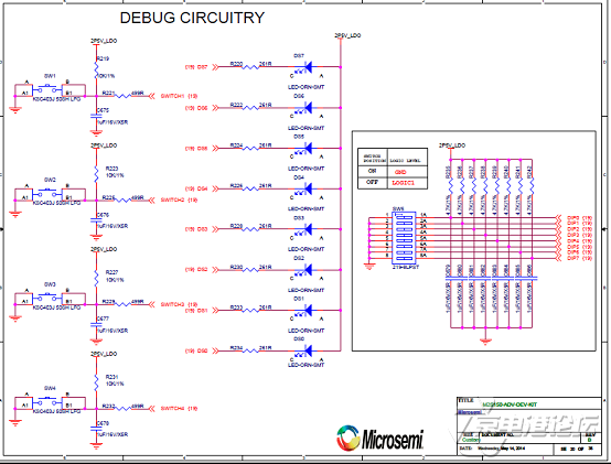
图20. SmartFusion2 SoC高级开辟板电路图(17)
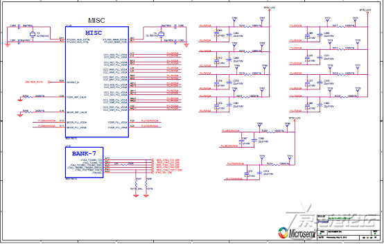
图21. SmartFusion2 SoC高级开辟板电路图(18)
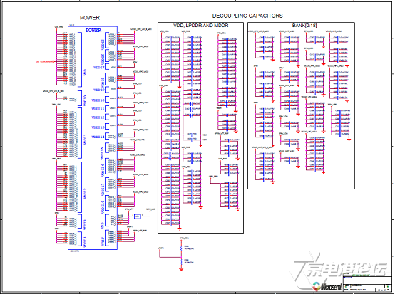
图22. SmartFusion2 SoC高级开辟板电路图(19)
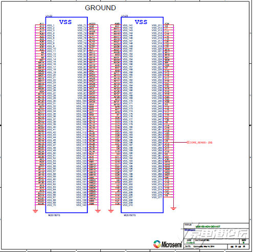
图23. SmartFusion2 SoC高级开辟板电路图(20)

图24. SmartFusion2 SoC高级开辟板电路图(21)

图25. SmartFusion2 SoC高级开辟板电路图(22)

图26. SmartFusion2 SoC高级开辟板电路图(23)
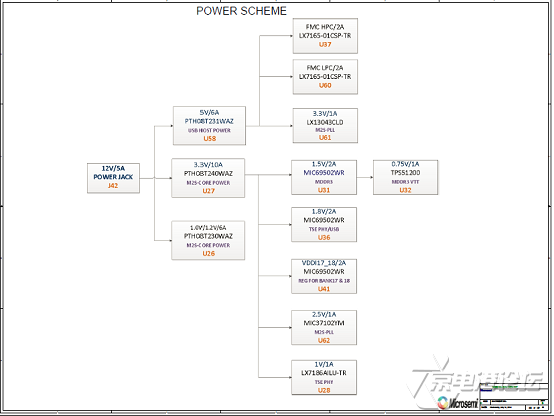
图27. SmartFusion2 SoC高级开辟板电路图(24)
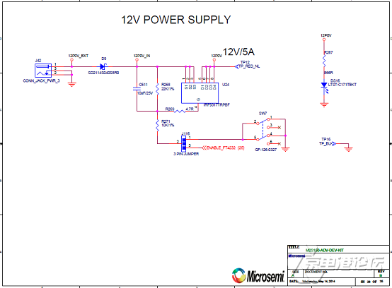
图28. SmartFusion2 SoC高级开辟板电路图(25)
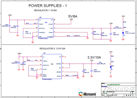
图29. SmartFusion2 SoC高级开辟板电路图(26)
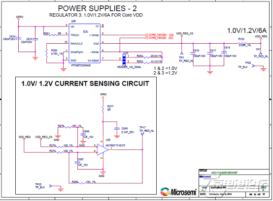
图30. SmartFusion2 SoC高级开辟板电路图(27)
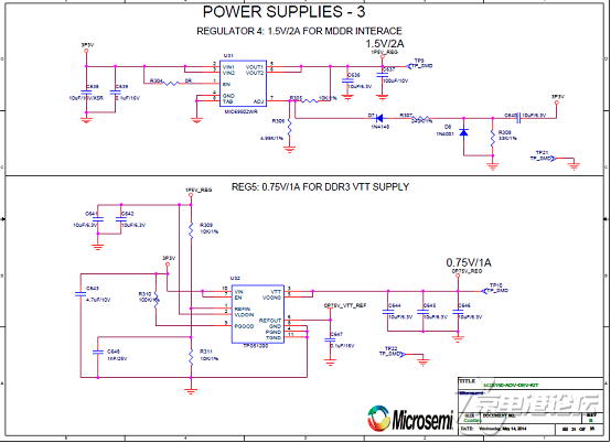
图31. SmartFusion2 SoC高级开辟板电路图(28)
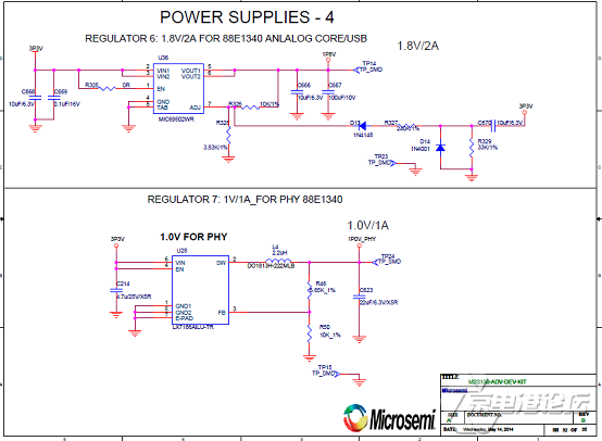
图32. SmartFusion2 SoC高级开辟板电路图(29)
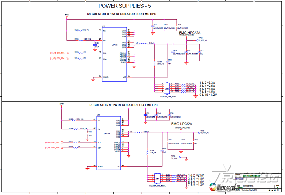
图33. SmartFusion2 SoC高级开辟板电路图(30)
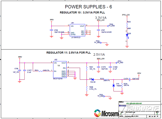
图34. SmartFusion2 SoC高级开辟板电路图(31)

图35. SmartFusion2 SoC高级开辟板电路图(32)
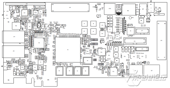
图36. SmartFusion2 SoC高级开辟板PCB元件结构图(顶层)

图37. SmartFusion2 SoC高级开辟板PCB元件结构图(底层)
SmartFusion2 SoC高级开辟板质料清单见:
 SmartFusion2 SoC高级开辟板质料清单.xls
详情请复制打开此衔接地址:
http://www.microsemi.com/products/fpga-soc/design-resources/dev-kits/smartfusion2/smartfusion2-advanced-development-kit#documents
 microsemi_smartfusion2_igloo2_datasheet_ds0128_v10.pdf


 热点图文
热点图文