NXP公司的LPC15xx系列产物是基于ARM Cortex-M3的非常低功耗的微控制器,工作频率高达72MHz,接纳3级流水线和哈佛架构,集成了多达256KB闪存,32KB ROM,4KB EEPROM和多达36KB SRAM,主要用在马达控制,马达控制,太阳能逆变器,家用电器,运动驱动,数字电源,修建物和工厂自动化以及工业和医疗.本文先容了LPC1549主要特点和优势,框架图,LPC1549马达控制板(永磁/Teknic马达)主要特点,框架图,电路图和PCB设计原理图.
The LPC15xx are ARM Cortex-M3 based microcontrollers for embedded applicationsfeaturing a rich peripheral set with very low power consumption. The ARM Cortex-M3 is a next generation core that offers system enhancements such as enhanced debug features and a higher level of support block integration.
The LPC15xx operate at CPU frequencies of up to 72 MHz. The ARM Cortex-M3 CPU incorporates a 3-stage pipeline and uses a Harvard architecture with separate local instruction and data buses as well as a third bus for peripherals. The ARM Cortex-M3 CPU also includes an internal prefetch unit that supports speculative branching.
The LPC15xx includes up to 256 kB of flash memory, 32 kB of ROM, a 4 kB EEPROM, and up to 36 kB of SRAM. The peripheral complement includes one full-speed USB 2.0 device, two SPI interfaces, three USARTs, one Fast-mode Plus I2C-bus interface, one C_CAN module, PWM/timer subsystem with four configurable, multi-purpose State Configurable Timers (SCTimer/PWM) with input pre-processing unit, a Real-time clock module with independent power supply and a dedicated oscillator, two 12-channel/12-bit, 2 Msamples/s ADCs, one 12-bit, 500 kSamples/s DAC, four voltage comparators with internal voltage reference, and a temperature sensor. A DMA engine can service most peripherals.
LPC1549主要特点和优势:
System:
ARM Cortex-M3 processor (version r2p1), running at frequencies of up to 72 MHz.
ARM Cortex-M3 built-in Nested Vectored Interrupt Controller (NVIC).
System tick timer.
Serial Wire Debug (SWD) with four breakpoints and two watchpoints.
Single-cycle multiplier supported.
Memory Protection Unit (MPU) included.
Memory:
Up to 256 kB on-chip flash programming memory with 256 Byte page write anderase.
Up to 36 kB SRAM.
4 kB EEPROM.
ROM API support:
Boot loader with boot options from flash or external source via USART, C_CAN, orUSB
USB drivers
ADC drivers
SPI drivers
USART drivers
I2C drivers
Power profiles and power mode configuration with low-power mode configuration option
DMA drivers
C_CAN drivers
Flash In-Application Programming (IAP) and In-System Programming (ISP).
Digital peripherals:
Simple DMA engine with 18 channels and 20 programmable input triggers.
High-speed GPIO interface with up to 76 General-Purpose I/O (GPIO) pins with configurable pull-up/pull-down resistors, open-drain mode, input inverter, and programmable digital glitch filter.
GPIO interrupt generation capability with boolean pattern-matching feature on eight external inputs.
Two GPIO grouped port interrupts.
Switch matrix for flexible configuration of each I/O pin function.
CRC engine.
Quadrature Encoder Interface (QEI).
Configurable PWM/timer/motor control subsystem:
Up to four 32-bit counter/timers or up to eight 16-bit counter/timers or combinationsof 16-bit and 32-bit timers.
Up to 28 match outputs and 22 configurable capture inputs with input multiplexer.
Up to 28 PWM outputs total.
Dither engine for improved average resolution of pulse edges.
Four State Configurable Timers (SCTimers) for highly flexible, event-driven timingand PWM applications.
SCT Input Pre-processor Unit (SCTIPU) for processing timer inputs and immediate
handling of abort situations.
Integrated with ADC threshold compare interrupts, temperature sensor, and analog comparator outputs for motor control feedback using analog signals.
Special-application and simple timers:
24-bit, four-channel, multi-rate timer (MRT) for repetitive interrupt generation at upto four programmable, fixed rates.
Repetitive interrupt timer for general purpose use.
Windowed Watchdog timer (WWDT).
High-resolution 32-bit Real-time clock (RTC) with selectable 1 s or 1 ms timeresolution running in the always-on power domain. RTC can be used for wake-upfrom all low power modes including Deep power-down.
Analog peripherals:
Two 12-bit ADC with up to 12 input channels per ADC and with multiple internaland external trigger inputs and sample rates of up to 2 Msamples/s. Each ADCsupports two independent conversion sequences. ADC conversion clock can bethe system clock or an asynchronous clock derived from one of the three PLLs.
One 12-bit DAC.
Integrated temperature sensor and band gap internal reference voltage.
Four comparators with external and internal voltage references (ACMP0 to 3).Comparator outputs are internally connected to the SCTimer/PWMs and ADCs and externally to pins. Each comparator output contains a programmable glitch filter.
Serial interfaces:
Three USART interfaces with DMA, RS-485 support, autobaud, and with synchronous mode and 32 kHz mode for wake-up from Deep-sleep and Power-down modes. The USARTs share a fractional baud-rate generator.
Two SPI controllers.
One I2C-bus interface supporting fast mode and Fast-mode Plus with data rates of up to 1Mbit/s and with multiple address recognition and monitor mode.
One C_CAN controller.
One USB 2.0 full-speed device controller with on-chip PHY.
Clock generation:
12 MHz internal RC oscillator trimmed to 1 % accuracy for 25 C Tamb +85 Cthat can optionally be used as a system clock.
Crystal oscillator with an operating range of 1 MHz to 25 MHz.
Watchdog oscillator with a frequency range of 503 kHz.
32 kHz low-power RTC oscillator with 32 kHz, 1 kHz, and 1 Hz outputs.
System PLL allows CPU operation up to the maximum CPU rate without the needfor a high-frequency crystal. May be run from the system oscillator or the internalRC oscillator.
Two additional PLLs for generating the USB and SCTimer/PWM clocks.
Clock output function with divider that can reflect the crystal oscillator, the mainclock, the IRC, or the watchdog oscillator.
Power control:
Integrated PMU (Power Management Unit) to minimize power consumption.
Reduced power modes: Sleep mode, Deep-sleep mode, Power-down mode, and Deep power-down mode.
APIs provided for optimizing power consumption in active and sleep modes and for configuring Deep-sleep, Power-down, and Deep power-down modes.
Wake-up from Deep-sleep and Power-down modes on activity on USB, USART,SPI, and I2C peripherals.
Wake-up from Sleep, Deep-sleep, Power-down, and Deep power-down modes from the RTC alarm or wake-up interrupts.
Timer-controlled self wake-up from Deep power-down mode using the RTC high-resolution/wake-up 1 kHz timer.
Power-On Reset (POR).
BrownOut Detect BOD).
JTAG boundary scan modes supported.
Unique device serial number for identification.
Single power supply 2.4 V to 3.6 V.
Temperature range 40 ℃ to +105 ℃.
Available as LQFP100, LQFP64, and LQFP48 packages.
LPC1549应用:
Motor control
Solar inverters
Motion drives
Home appliances
Digital power supplies
Building and factory automation
Industrial and medical
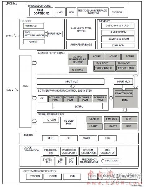
图1.LPC15xx框架图
LPC1549马达控制板(永磁/Teknic马达)
LPC1549 Motor Control Kit (Permanent Magnet/Teknic Motor) makes it possible for you to get started with motor control prototyping immediately. It is a platform for low voltage motor control based on NXP’s MCUs. With this universal platform it is possible to control motors.
The LPC1549 PMSM motor control solution provides a Field-Oriented Control (FOC) example to get you started with motor control prototyping. This example utilizes the QEI feature on the LPC1500 to monitor the position and velocity of the motor for both sensor and sensorless modes. The additional advanced features of the LPC1500 including the SCTimer/PWM and high speed ADC ensures easy and reliable control of time critical peripherals, and a mechanism for sychronization of the ADC’s with the PWM for exact timing of the sample moments.
FOC is a more advanced approach where each phase is driven sinusoidally and permanently powered so the magnetic field inside the motor is regulated to the most optimal value. The project is implemented on the LPC1549 PMSM Motor Control Kit, which includes an LPC1549 LPCXpresso board.
Download package include firmware source code and an application note which describes the sensored motor control operation using the QEI and SCTimer/PWM in detail. You can download package from bottom of this page.FOC Control Block Diagram
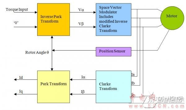
图2.FOC控制框架图
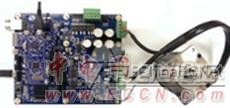
图3.LPC1549马达控制板(永磁/Teknic马达)外形图
LPC1549马达控制板(永磁/Teknic马达)主要特点:
The LPC1549 ARM Cortex-M3 based microcontroller 256 kB of flash memory, 32 kB of ROM, 4 kB EEPROM, and up to 36 kB of SRAM Expansion connector for control by LPC1800/LPC4000/LPC2900 families, or other 4 phases (based on NXP PSMN2R6-40YS N-channel MOSFET), accessed via screw terminals Phase control support 100% duty cycle Voltage measurement (on three phases and virtual ground)Current measurement (in-phase on three phases and common low-side)Input current measurement, including over-current trip Break functionality Hall & QEI sensor inputs, connected via screw terminals
Temperature sensor
12-30 V input voltage, 17 A max current (max 300 W output)
On-board 15 W power supply (+11 V, +5 V, +3.3 V)
USB interface (must be supported by controlled MCU)
Ethernet interface (must be supported by controlled MCU)
CAN interface (must be supported by controlled MCU)
RS422/485 interface
UART-to-USB interface
5-key joystick switch
96 x 64 pixel OLED
Reset pushbutton
I²C-EEPROM
SWD/JTAG connector
2.1 mm input jack, or via screw terminals
12-30 V, 17 A max
Demo Box Contents
LPCXpresso Motor Control Board, rev. B
LPCXpresso LPC1549 Board
Permanent Magnet/Teknic Motor
24 V Power supply
mini-B to A USB cable
micro-B to A USB cable
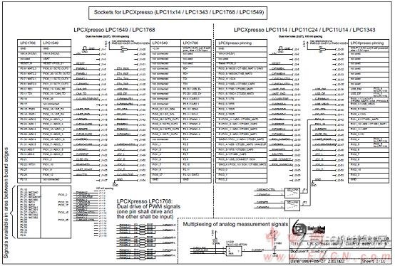
图4.LPC1549马达控制板(永磁/Teknic马达)电路图(1)
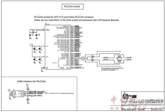
图5.LPC1549马达控制板(永磁/Teknic马达)电路图(2)
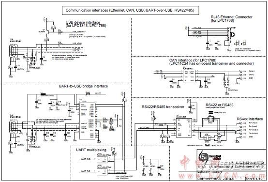
图6.LPC1549马达控制板(永磁/Teknic马达)电路图(3)
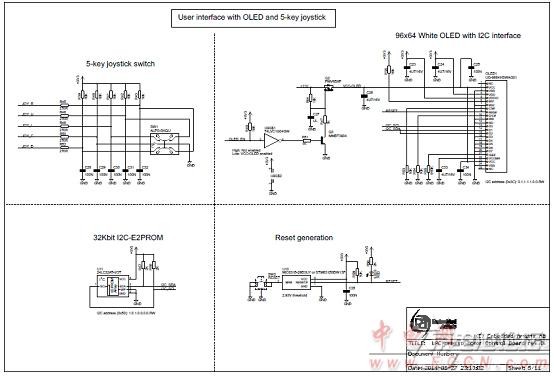
图7.LPC1549马达控制板(永磁/Teknic马达)电路图(4)

图8.LPC1549马达控制板(永磁/Teknic马达)电路图(5)
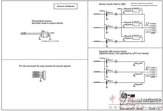
图9.LPC1549马达控制板(永磁/Teknic马达)电路图(6)
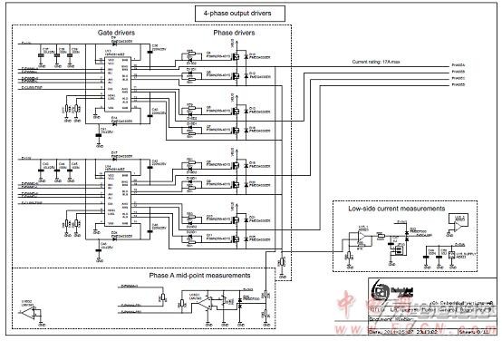
图10.LPC1549马达控制板(永磁/Teknic马达)电路图(7)
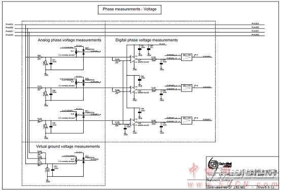
图11.LPC1549马达控制板(永磁/Teknic马达)电路图(8)
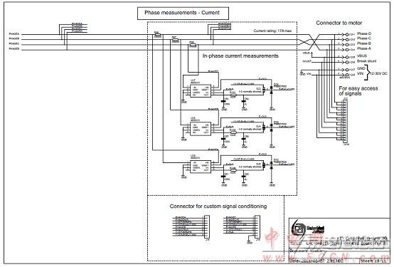
图12.LPC1549马达控制板(永磁/Teknic马达)电路图(9)
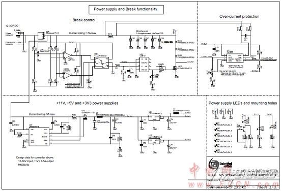
图13.LPC1549马达控制板(永磁/Teknic马达)电路图(10)
详情请复制打开此衔接地址:
http://www.nxp.com/documents/data_sheet/LPC15XX.pdf
和http://www.nxp.com/documents/user_manual/UM10736.pdf
以及http://www.nxp.com/documents/design_support/OM13067_OM13068_Schematic_File.pdf
 LPC15XX.pdf
UM10736.pdf


 热点图文
热点图文