|
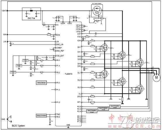
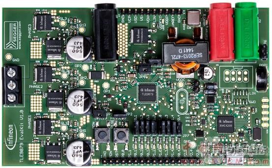
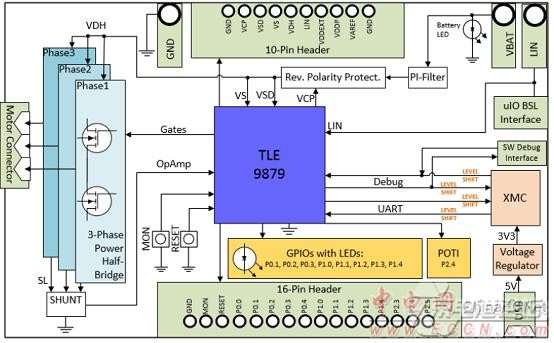
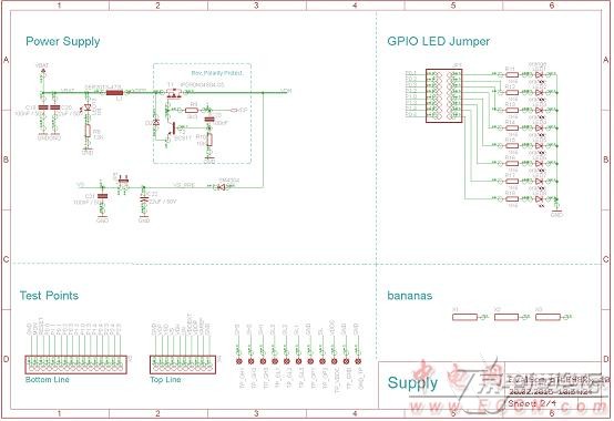
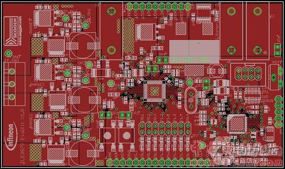
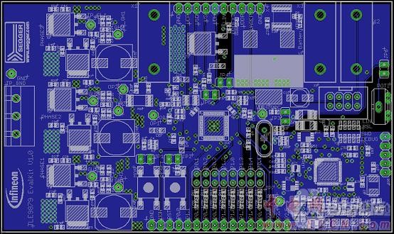
infineon公司的TLE9879是集成了LIN 2.2与SAEJ2602兼容的LIN收发器和BLDC MOSFET驱动器的微控制器,接纳尺度的ARM® Cortex™ M3内核,包罗了六个全集成的NFET驱动器,适合通过外接六个功率NFET来驱动3相马达,主要用于汽车的燃料泵,HVAC,引擎冷却风扇,水泵和BLDC蚌与风扇.本文先容了TLE9879主要特点,框架图,BLDC马达驱动电路和质料清单,以及评估板TLE9879 EVALKIT,电路图和PCB设计文件图. Microcontroller with LIN and BLDC MOSFET Driver for Automotive Applications The TLE9879QXA20 is part of the TLE987x product family. The TLE9879QXA20 is a single chip 3-Phase motor driver that integrates the industry standard ARM® Cortex™ M3 core, enabling the implementation of advanced motor control algorithms such as field-oriented control. It includes six fully integrated NFET drivers optimized to drive a 3-Phase motor via six external power NFETs, a charge pump enabling low voltage operation and programmable current along with current slope control for optimized EMC behavior. Its peripheral set includes a current sensor, a successive approximation ADC synchronized with the capture and compare unit for PWM control and 16-bit timers. A LIN transceiver is also integrated to enable communication to the device along with a number of general purpose I/Os. It includes an on-chip linear voltage regulator to supply external loads. It includes an on-chip linear voltage regulator to supply external loads. It is a highly integrated automotive qualified device enabling cost and space efficient solutions for mechatronic BLDC motor drive applications such as pumps and fans. TLE9879主要特点: Six current programmable Drivers with charge pump for N-Channel MOSFET TLE9879目标应用: Fuel pump 评估板TLE9879 EVALKIT All relevant chip pins are connected to pin headers at the edge of the board, where signals can be probed or applied directly (see Table 2, Table 3). By different jumper settings LEDs can be put in parallel to several ports and selected functions can be configured (see Table 6). Push button switches allow easy hardware reset and triggering of the MON input. There are intended test points for all six gate driver pins, for measurements at the shunt, VDDC and several ground points on the evaluation board (see Figure 3). For testing analog signals ADC inputs can be varied by the potentiometer on board. Three phases of motor current can be picked off at a terminal block to connect a DC brushless motor. The evaluation board can be operated by standard laboratory equipment as power supply and LIN communication are working via banana jacks. Debugging and UART are provided via an USB interface combined with onboard Segger J-Link (XMC4200). Bidirectional level shifters ensure that the respective XMC pins are in tristate as long as UART or debugging is not used. In case the user wants to use another ISP than the onboard Segger the SWD interface can be used. To program the TLE9879 via LIN there is an additional uIO BSL interface (see Table 4). There is a battery LED that indicates that the board is connected to supply the right way. Otherwise reverse polarity protection secures the board from damage by cross connection.
|


 Infineon-TLE9879QXA20-DS-v01_00-EN.pdf


 热点图文
热点图文