ADI公司的ADSP-CM40x系列是基于ARM® Cortex-M4TM内核的混淆信号控制处理器,浮点运算单位工作频率高达240MHz,集成了高达384KB SRAM,2MB 闪存,加快器和最适适用来控制马达和光伏(PV)逆变器控制的外设以及有两个16位SAR型ADC和两个12位DAC组成的模拟模块,单电源工作,主要用在马达控制,嵌入式工业应用,仪器仪表,医疗和消费类电子.本文先容了ADSP-CM40x主要特点和框架图, 模拟子系统框架图以及Cortex-M4内核特点和框架图, ADSP-CM408F EZ-KIT Lite®评估板主要特点和框架图,电路图和质料清单.
The ADSP-CM40x family of mixed-signal control processors is based on the ARM® Cortex-M4TM processor core with floatingpoint unit operating at frequencies up to 240 MHz and integrating up to 384KB of SRAM memory, 2MB of flash memory, accelerators and peripherals optimized for motor control and photo-voltaic (PV) inverter control and an analog module consisting of two 16-bit SAR-type ADCs and two 12-bit DACs. The ADSP-CM40x family operates from a single voltage supply (VDD_EXT/VDD_ANA), generating its own internal voltage supplies using internal voltage regulators and an external pass transistor.
This family of mixed-signal control processors offers low static power consumption and is produced with a low-power and low voltage design methodology, delivering world class processor and ADC performance with lower power consumption.
By integrating a rich set of industry-leading system peripherals and memory, the ADSP-CM40x mixed-signal control processors are the platform of choice for next-generation applications that require RISC programmability, advanced communications and leading-edge signal processing in one integrated package. These applications span a wide array of markets including power/motor control, embedded industrial, instrumentation, medical and consumer.
Each ADSP-CM40x family member contains the following modules.
• 8 GP timers with PWM output
• 3-Phase PWM units with up to 4 output pairs per unit
• 2 CAN modules
• 1 two-wire interface (TWI) module
• 3 UARTs
ADSP-CM40x主要特点:
100 MHz to 240 MHz ARM Cortex-M4 with floating-point unit
128K Byte to 384K Byte zero-wait-state L1 SRAM with
16K Byte L1 cache
Up to 2M Byte flash memory
16-bit asynchronous external memory interface
Enhanced PWM units
Four 3rd/4th order SINC filters for glueless connection of isolated ADCs
Harmonic analysis engine
10/100 Ethernet MAC
Full Speed USB On-the-Go (OTG)
Two CAN (controller area network) 2.0B interfaces
Three UART ports
Two Serial Peripheral Interface (SPI-compatible) ports
Eight 32-bit general-purpose timers
Four Encoder Interfaces, 2 with frequency division
Single power supply
176-lead (24 mm × 24 mm) RoHS compliant LQFP package
120-lead (14 mm × 14 mm) RoHS compliant LQFP package
ANALOG SUBSYSTEM FEATURES
ADC controller (ADCC) and DAC controller (DACC)
Two 16-bit SAR ADCs with up to 24 multiplexed inputs,supporting dual simultaneous conversion in 380 ns (16-bit, no missing codes, ±3.5LSB INL)
Two 12-bit R-string DACs, with output rate up to 50 kHz
Two 2.5 V precision voltage reference outputs
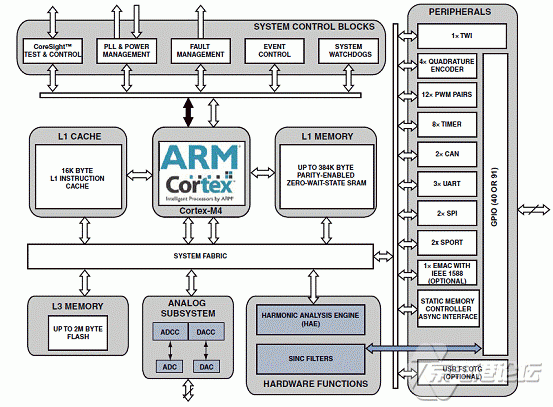
图1{京电港论坛}.ADSP-CM40x系列框架图
模拟子系统
The processors contain two ADCs and two DACs. Control of these data converters is simplified by a powerful on-chip analog- to-digital conversion controller (ADCC) and a digital-to analog conversion controller (DACC). The ADCC and DACC are integrated seamlessly into the software programming model, and they efficiently manage the configuration and real-time operation of the ADCs and DACs.
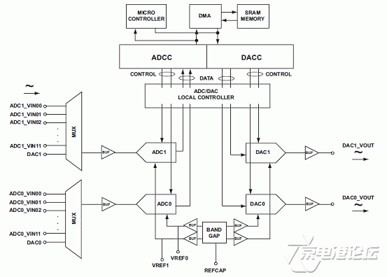
图2{京电港论坛}.CM407F/CM408F模拟子系统框架图
ARM CORTEX-M4核
The ARM Cortex-M4 is a 32-bit reduced instruction set computer (RISC). It uses a single 32-bit bus for instruction and data. The length of the data can be eight bits, 16 bits, or 32 bits. The length of the instruction word is 16 or 32 bits. The controller has the following features.
Cortex-M4 Architecture
• Thumb-2 ISA Technology
• DSP and SIMD extensions
• Single cycle MAC (Up to 32 × 32 + 64 -> 64)
• Hardware Divide Instructions
• Single-precision FPU
• NVIC Interrupt Controller (129 Interrupts and 16 Priorities)
• Memory Protection Unit (MPU)
• Full CoreSightTM Debug, Trace, Breakpoints, Watchpoints, and Cross-Triggers
Microarchitecture
• 3-stage pipeline with branch speculation
• Low-latency interrupt processing with tail chaining
Configurable For Ultra Low Power
• Deep sleep mode, dynamic power management
• Programmable Clock Generator Unit
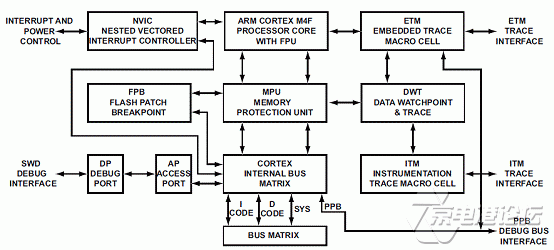
图3{京电港论坛}. Cortex-M4内核框架图
ADSP-CM408F EZ-KIT Lite®评估系统
The evaluation board is designed to be used in conjunction with the IAR Embedded Workbench development tools to test capabilities of the ADSP-CM408F processors. The development environment aids advanced application code development and debug, such as:
• Create, compile, assemble, and link application programs written in C++, C, and assembly
• Load, run, step, halt, and set breakpoints in application programs
• Read and write data and program memory
• Read and write core and peripheral registers
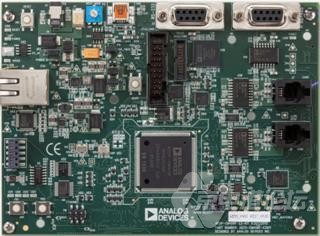
图4{京电港论坛}. ADSP-CM408F EZ-KIT Lite®评估板外形图
ADSP-CM408F EZ-KIT Lite®评估板主要特点:
• Analog Devices ADSP-CM408F processor
• 176-pin LQFP package
• 30 MHz CLKIN core oscillator
• SRAM memory (SMC0) chip
• 256K x 16-bit (4M bit)
• Cypress CY7C1041DV33
• Ethernet PHY (ETH0)
• 10/100 Mb/s
• Texas Instruments DP83848C
• Universal Asynchronous Receiver/Transmitter (UART0)
• Analog Devices ADM3252E RS-232 line transceiver
• DB9 female connector
• Universal Asynchronous Receiver/Transmitter (UART1)
• Analog Devices ADM2682E RS-485 line transceiver
• DB9 female connector
• Controller Area Network (CAN) interfaces
• CAN0―Analog Devices ADM3053 transceiver and RJ11 connector
• CAN1―Analog Devices ADM3053 transceiver and RJ11 connector
• USB interface
• Molex 56579-0576 connector
• Display
• New Haven NHD-0220D3Z-FL-GBW
• 2 x 20 character
• 2-wire interface (TWI) control
• RESET controller
• Analog Devices ADM708 microprocessor supervisory circuits
• Debug (JTAG/SWD/SWV/TRACE) interface
• JTAG/SWD 20-pin 0.1” header for use with IAR emulators
• Trace/JTAG/SWD/SWV 20-pin 0.05” header
• LEDs
• Eight LEDs: one power (green), one board reset (red), one Ethernet speed (green), one SYS_FAULT (red), and four general-purpose (amber)
• Push buttons
• Four push buttons: one reset, one wake, two IRQ/Flag
• Asynchronous connector
• 180-pin Samtec (QSH-090-01-F-D-A) 0.5 mm spacing
• SMC0 address, data, and control
• CLKOUT
• SPI1
• UART2
• TWI0
• GPIOs
• RESET
• GND/3.3V/5V output
• Pulse-width modulation (PWM) connector
• 180-pin Samtec (QSH-090-01-F-D-A) 0.5 mm spacing
• PWM0―PWM2
• SINC0
• SPI1
• SPT0
• TWI0
• TMR0
• CNT0―CNT3
• GPIO
• RESET
• GND/3.3V/5V output
• 5V output
• Analog connector interface
• 120-pin Samtec (QSH-060-01-F-D-A) 0.5 mm spacing
• ADC0
• AGND/GND/VREF/5VOUT
• ADR441 voltage reference (VREF)
• ADA4899 buffer―0.1” header for reference
• 1588 connector
• 0.1” header 6-pin
• External power supply
• CE compliant
• 5V @ 3.6 Amps
• Ability to power from the PWM connector
• Other features
• 0.05-ohm resistors for processor current measurement
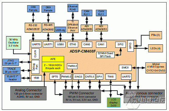
图5{京电港论坛}. ADSP-CM408F EZ-KIT Lite®评估板框架图
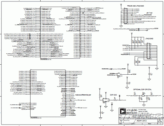
图6{京电港论坛}. ADSP-CM408F EZ-KIT Lite®评估板电路图(1)
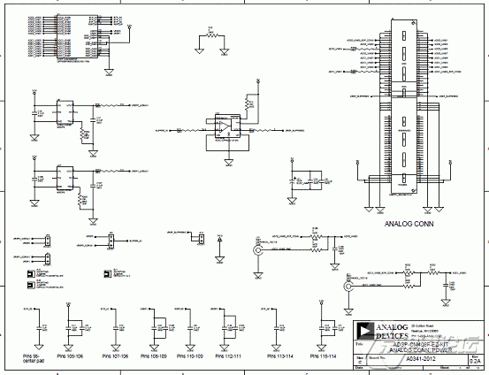
图7{京电港论坛}. ADSP-CM408F EZ-KIT Lite®评估板电路图(2)
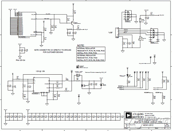
图8{京电港论坛}. ADSP-CM408F EZ-KIT Lite®评估板电路图(3)
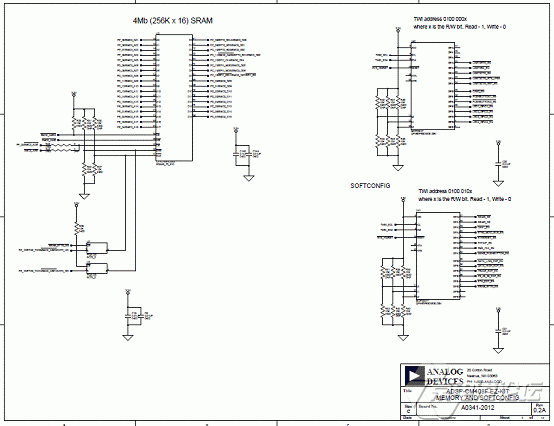
图9{京电港论坛}. ADSP-CM408F EZ-KIT Lite®评估板电路图(4)
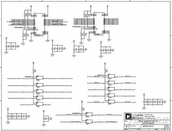
图1{京电港论坛}0. ADSP-CM408F EZ-KIT Lite®评估板电路图(5)

图1{京电港论坛}1. ADSP-CM408F EZ-KIT Lite®评估板电路图(6)
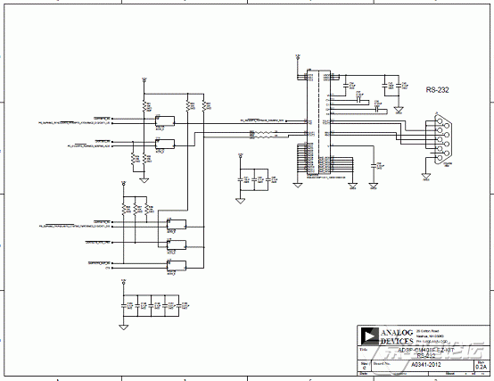
图1{京电港论坛}2. ADSP-CM408F EZ-KIT Lite®评估板电路图(7)
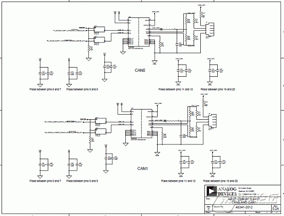
图1{京电港论坛}3. ADSP-CM408F EZ-KIT Lite®评估板电路图(8)

图1{京电港论坛}4. ADSP-CM408F EZ-KIT Lite®评估板电路图(9)
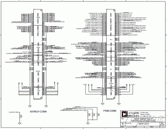
图1{京电港论坛}5. ADSP-CM408F EZ-KIT Lite®评估板电路图(10)

图1{京电港论坛}6. ADSP-CM408F EZ-KIT Lite®评估板电路图(11)
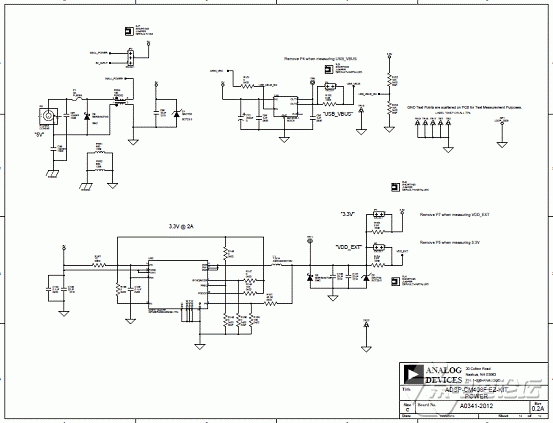
图1{京电港论坛}7. ADSP-CM408F EZ-KIT Lite®评估板电路图(12)
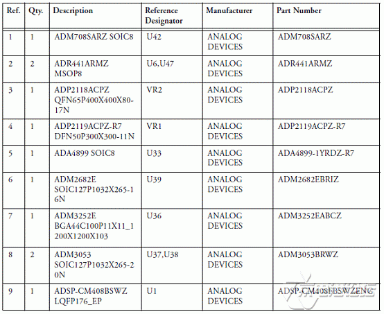
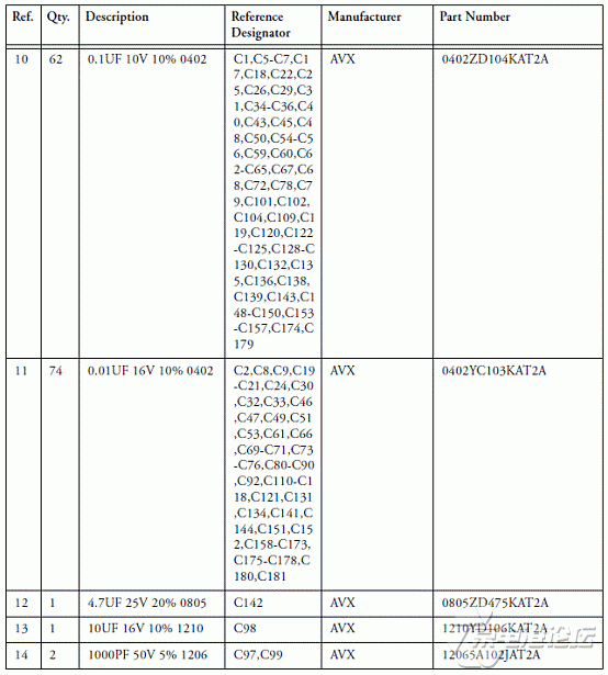
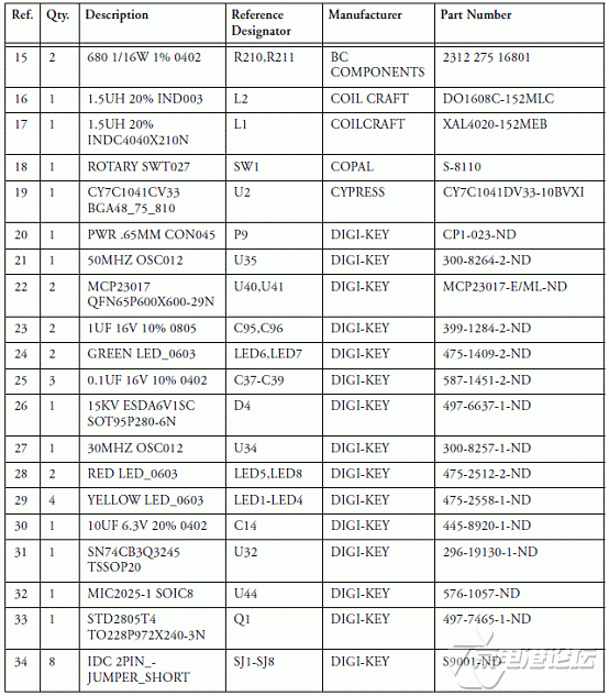
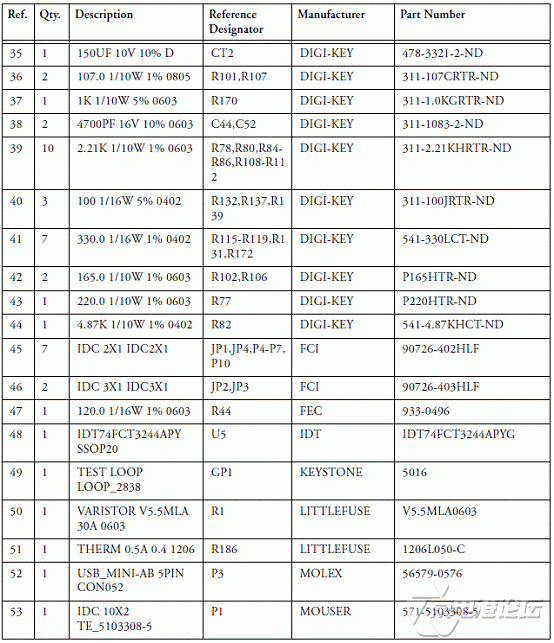
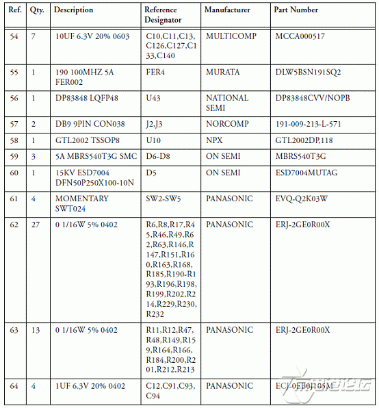
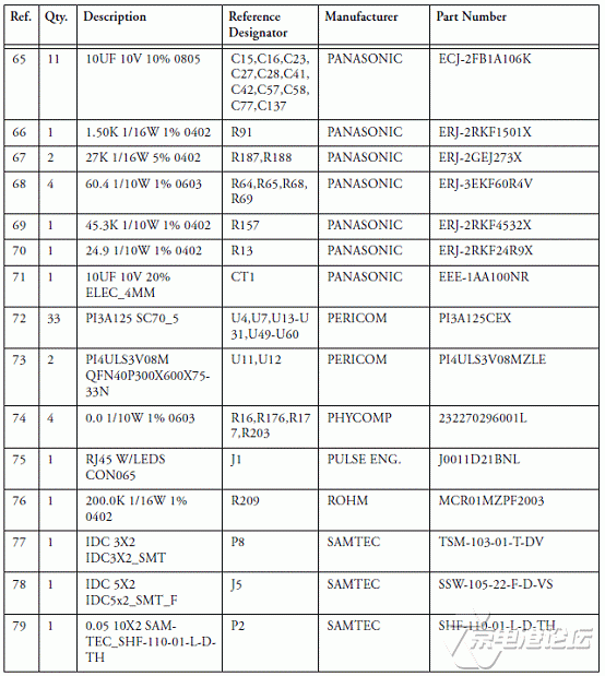
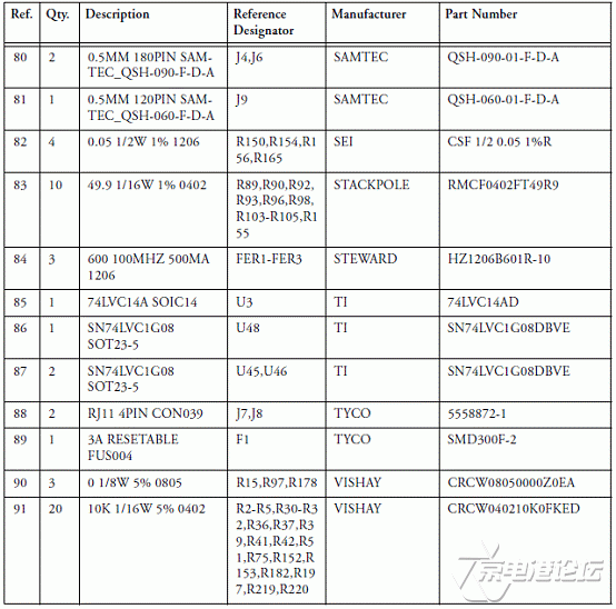
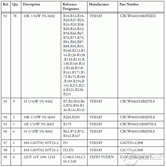
ADSP-CM408F EZ-KIT Lite®评估板质料清单:
详情请复制打开此衔接地址:
http://www.analog.com/static/imported-files/data_sheets/ADSP-CM402F_CM403F_CM407F_CM408F.pdf
和http://www.analog.com/static/imported-files/eval_kit_manuals/ADSP-CM408F_ezkit_rev.1.1.pdf
 ADSP-CM402F_CM403F_CM407F_CM408F.pdf
ADSP-CM408F_ezkit_rev.1.1.pdf


 热点图文
热点图文