|
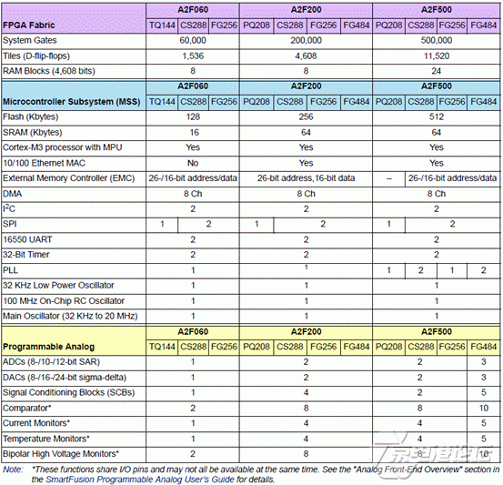
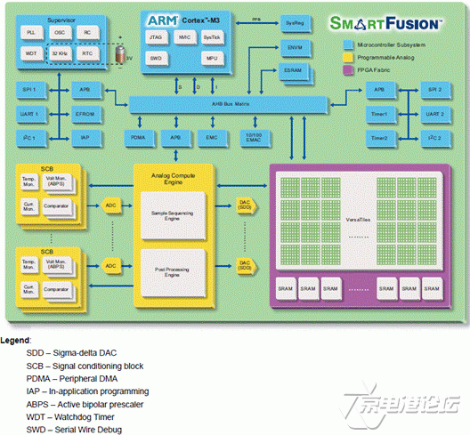
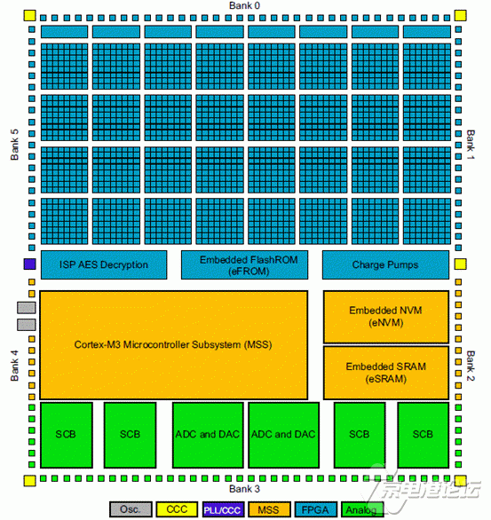
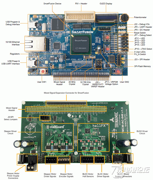
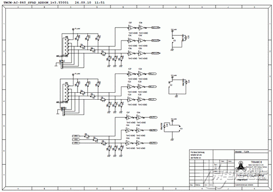
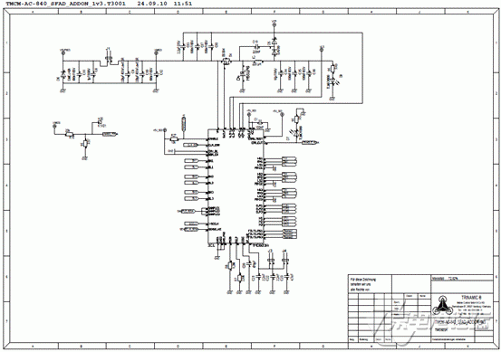
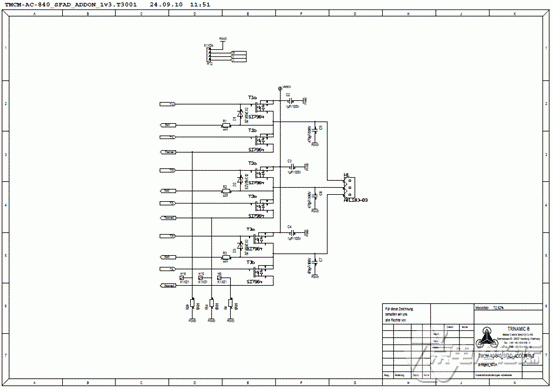
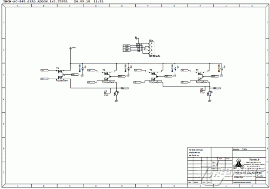
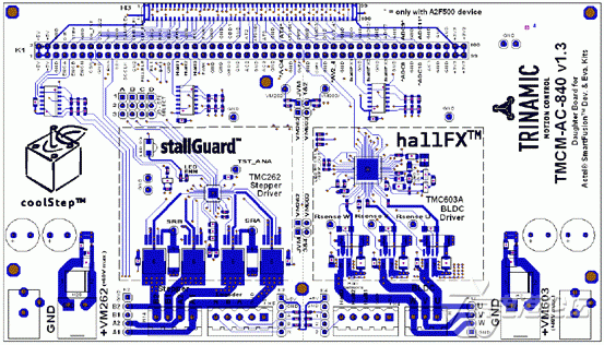
Microsemi 公司的SmartFusion双马达控制套件包罗SmartFusion 评估板和与之配对的TRINAMIC公司的TMCM-AC-840子板,能为步进马达和无刷DC马达(BLDC)提供定制化片上系统(cSoC)马达控制平台,而SmartFusion cSoC器件集成了FPGA,ARM® Cortex™-M3处理器,以及可编程的模拟,提供完全定制的IP掩护和容易使用;别的还集成了SRAM存储器和SPI闪存.本京电港论坛文章先容了SmartFusion cSoC主要特点,方框架图和系统架构图,BLDC和步进马达演示设计根本框架图以及SmartFusion双马达控制套件主要特点,SmartFusion 评估板主要特点,以及TMCM-AC-840子板主要特点,电路原理图纸和马达控制子板PCB线路板结构图. The SmartFusion® family of cSoCs builds on the technology first introduced with the Fusion mixed signal FPGAs. SmartFusion cSoCs are made possible by integrating FPGA technology with programmable high-performance analog and hardened ARM Cortex-M3 microcontroller blocks on a flash semiconductor process. The SmartFusion cSoC takes its name from the fact that these three discrete technologies are integrated on a single chip, enabling the lowest cost of ownership and smallest footprint solution to you. SmartFusion定制片上系统(cSoC)主要特点: Microcontroller Subsystem (MSS) • Hard 100 MHz 32-Bit ARM® Cortex™-M3 C 1.25 DMIPS/MHz Throughput from Zero Wait State Memory C Memory Protection Unit (MPU) C Single Cycle Multiplication, Hardware Divide C JTAG Debug (4 wires), Serial Wire Debug (SWD, 2 wires), and Single Wire Viewer (SWV) Interfaces • Internal Memory C Embedded Nonvolatile Flash Memory (eNVM), 128 Kbytes to 512 Kbytes C Embedded High-Speed SRAM (eSRAM), 16 Kbytes to 64 Kbytes, Implemented in 2 Physical Blocks to Enable Simultaneous Access from 2 Different Masters • Multi-Layer AHB Communications Matrix C Provides up to 16 Gbps of On-Chip Memory Bandwidth,1 Allowing Multi-Master Schemes • 10/100 Ethernet MAC with RMII Interface2 • Programmable External Memory Controller, Which Supports: C Asynchronous Memories C NOR Flash, SRAM, PSRAM C Synchronous SRAMs • Two I2C Peripherals • Two 16550 Compatible UARTs • Two SPI Peripherals • Two 32-Bit Timers • 32-Bit Watchdog Timer • 8-Channel DMA Controller to Offload the Cortex-M3 from Data Transactions • Clock Sources C 32 KHz to 20 MHz Main Oscillator C Battery-Backed 32 KHz Low Power Oscillator with Real-Time Counter (RTC) C 100 MHz Embedded RC Oscillator; 1% Accurate C Embedded Analog PLL with 4 Output Phases (0, 90, 180, 270) High-Performance FPGA • Based on proven ProASIC®3 FPGA Fabric • Low Power, Firm-Error Immune 130-nm, 7-Layer Metal, Flash-Based CMOS Process • Nonvolatile, Live at Power-Up, Retains Program When Powered Off • 350 MHz System Performance • Embedded SRAMs and FIFOs C Variable Aspect Ratio 4,608-Bit SRAM Blocks C x1, x2, x4, x9, and x18 Organizations C True Dual-Port SRAM (excluding x18) C Programmable Embedded FIFO Control Logic • Secure ISP with 128-Bit AES via JTAG • FlashLock® to Secure FPGA Contents • Five Clock Conditioning Circuits (CCCs) with up to 2 Integrated Analog PLLs C Phase Shift, Multiply/Divide, and Delay Capabilities C Frequency: Input 1.5C350 MHz, Output 0.75 to 350 MHz Programmable Analog Analog Front-End (AFE) • Up to Three 12-Bit SAR ADCs C 500 Ksps in 12-Bit Mode C 550 Ksps in 10-Bit Mode C 600 Ksps in 8-Bit Mode • Internal 2.56 V Reference or Optional External Reference • One First-Order ΣΔ DAC (sigma-delta) per ADC C 8-Bit, 16-Bit, or 24-Bit 500 Ksps Update Rate • Up to 5 High-Performance Analog Signal Conditioning Blocks (SCB) per Device, Each Including: C Two High-Voltage Bipolar Voltage Monitors (with 4 input ranges from ±2.5 V to C11.5/+14 V) with 1% Accuracy C High Gain Current Monitor, Differential Gain = 50, up to 14 V Common Mode C Temperature Monitor (Resolution = ¼°C in 12-Bit Mode; Accurate from C55°C to 150°C) • Up to Ten High-Speed Voltage Comparators (tpd = 15 ns) Analog Compute Engine (ACE) • Offloads Cortex-M3CBased MSS from Analog Initialization and Processing of ADC, DAC, and SCBs • Sample Sequence Engine for ADC and DAC Parameter Set-Up • Post-Processing Engine for Functions such as Low-Pass Filtering and Linear Transformation • Easily Configured via GUI in Libero® Integrated Design (IDE) Software I/Os and Operating Voltage • FPGA I/Os C LVDS, PCI, PCI-X, up to 24 mA IOH/IOL C Up to 350 MHz • MSS I/Os C Schmitt Trigger, up to 6 mA IOH, 8 mA IOL Up to 180 MHz • Single 3.3 V Power Supply with On-Chip 1.5 V Regulator • External 1.5 V Is Allowed by Bypassing Regulator (digital VCC = 1.5 V for FPGA and MSS, analog VCC =3.3 V and 1.5 V) SmartFusion系列产物: SmartFusion双马达控制套件 Microsemi’s SmartFusion Dual Motor Control Kit features a SmartFusion evaluation board paired with TRINAMIC’s TMCM-AC-840 Daughter Board to provide a customizable system-on-chip (cSoC) motor control prototyping platform for stepper and brushless DC motors (BLDC). One of each type of motor is included along with necessary cables and power supplies. SmartFusion cSoCs are the only devices that integrate an FPGA, an ARM® Cortex™-M3 processor, and programmable analog, offering full customization, IP protection, and ease- of-use. The device contains on-chip flash and on-chip SRAM memory, as well as additional SPI flash memory on the board. SmartFusion FPGA fit well to motion control applications. Due to the combination of hardware, software, and additional analog components complex systems can be integrated within a single chip. This drastically reduces the number of required components to realize a motion control unit. Real time critical tasks can be implemented in hardware. Complex - but less real time critical tasks - can be realized in software. Real Time critical tasks are commutation of fast rotating BLDC motors or processing of high resolution encoder signals. Processing of analog signals, e.g., voltage and current measurement is a typical task in motion control applications. Therefore, the SmartFusion’s. analog I/Os and processing functionality can be used. SmartFusion 评估板主要特点: • Supports SmartFusion evaluation,including ARM Cortex-M3, FPGA and programmable analog • Free one-year Libero Integrated Design Environment (IDE) software and Gold license with SoftConsole for embedded design • Two USB cables • Online user’s guide, tutorial and design examples • Printed circuit board (PCB线路板) schematics, layout fi les and bill-of-materials (BOM) • Board features - Ethernet interface - USB port for power and HyperTerminal - USB port for programming and debug - J-Link header for debug - Mixed signal header - SPI fl ash C off-chip memory - Reset and 2 user switches, 8 LEDs - POT for voltage / current monitor - Temperature monitor - Organic light-emitting diode (OLED) Together with Trinamic’s integrated BLDC motor gate driver TMC603A (or with the integrated stepper motor driver TMC262), one can realize a power stage with a couple of components as demonstrated with the TMCM-AC-840 Daughter Board Kit for direct plug to the ACTEL SmartFusion. Evaluation Kit boards or Development Kit boards. The TRINAMIC TMCM-AC-840 Daughter Board Kit is a power driver for brushless DC motors (BLDC) as well as stepper motors. The TMCM-AC-840 Daughter Board Kit incorporates one TMC603A BLDC motor driver IC and one TMC262 coolStep. stepper motor driver IC as well as two motors (one BLDC and one stepper motor) and a fitting portable power supply to start right away. The TMCM-AC-840 is designed to operate with the ACTEL SmartFusion. Development Kit (Revision C and later) as well as the ACTEL SmartFusion. Evaluation Kit as both boards are pin-compatible regarding their Mixed Signal Expansion Header (see the ACTEL user guides for both boards). When using the TMCM-AC-840 in combination with an ACTEL SmartFusion. Development Kit that is equipped with the larger A2F500 SmartFusion. FPGA, some additional analog I/Os are available on the Mixed Signal Header. All signals of the Mixed Signal Expansion Header are easily accessible via pin headers on the TMCM-AC-840 daughter board. TMCM-AC-840子板主要特点: One BLDC motor pre-driver TMC603A o Integrated dual range high precision current measurement amplifiers o Supports shunt less current measurement using power MOS transistor RDSon o hallFX™sensorless back EMF commutation emulates hall sensors o Integrated break-before-make logic: No special microcontroller PWM hardware required o See the TMC603A datasheet for more information [2] One stepper motor driver TMC262 o Energy saving high resolution microstepping two phase stepper driver with step and direction interface and external power stage o High precision sensor-less motor load measurement stallGuard2™ o Energy efficiency and coolness by automatic load dependant motor current regulation technology coolStep™ Save up to 75% of energy! o See the TMC262 datasheet for more information [3] One BLDC Motor (Qmot QBL4208-41-04-006) o Maximum rated current 1.8A, peak current 5.4A, see motor spec/user guide for more information on electrical and mechanical parameters [6] One Stepper Motor (Qmot QSH4218-35-10-027) o Maximum current 1.0A, see motor spec/user guide for more information on electrical and mechanical parameters [5] One portable power supply with international connectors, 24V/1A (version 1.3 and higher) Hard top case for easy handling and safe transport (version 1.3 and higher) The Board and the driver stages support maximum motor currents of up to 2A for stepper driver block and up to 4A (5A with good cooling) for the BLDC driver block. Easy plug and play solution using the freely available demo design (under BSD) for the BLDC and stepper functionality Hall-sensor interface for BLDC motors ABN encoder interface for high precision position measurement o The encoder interface can be used with the stepper or with the BLDC motor. Various analog signals connected to the analog blocks (Signal Conditioning Blocks, SCBs) of the Actel SmartFusion™Device for, e.g., voltage measurement Additional RSENSE measurement pins All signals of the Mixed Signal Expansion Header can be accessed via additional pin headers for test and measurement Parallel operation of BLDC and stepper motor driver Pin-compatible to both the Actel SmartFusion™Development Kit as well as the Actel SmartFusion™Evaluation Kit Each driver requires a separate DC supply voltage o The stepper driver block (TMC262): +VM262 = 12V to 40V o The BLDC driver block (TMC603A): +VM603 = 12V to 48V o Using jumpers, a single power supply can be used for both drivers SmartFusion双马达控制套件包罗: For this demonstration design, the SmartFusion Dual Motor Control Kit comes with the following: • SmartFusion Evaluation Kit board • Trinamic TMCM-AC-840 daughter board kit (including 2 motors) • 2 USB cables for programming and UART connection to your workstation • Microsemi Libero® software tool chain • FlashPro programming software • 1 power supply unit For each motor block (stepper or BLDC) you need a separate power supply unit C With only one power supply you can only drive one motor at a time
上:SmartFusion评估板;下:TMCM-AC-840马达控制子板
|


 热点图文
热点图文