|
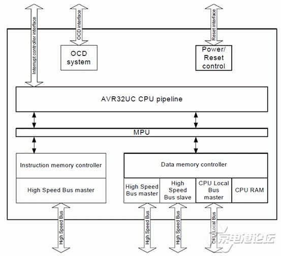
Atmel 公司的AT32UC3C是{方案}AVR32UC RISC处理器的系统级芯片(SoC)的高性能32位微控制器,工作频率高达66MHz,具有1.49 DMIPS / MHz的性能,存储器掩护单位(MPU),快速和机动的中断控制器,支持今世操纵系统和实时操纵系统.器件集成了闪存和SRAM存储器,主要用在马达控制如HVAC,门,窗户和座椅的直接马达控制以及车内通信的CAN,LIN接口等.本京电港论坛文章先容了AT32UC3C主要特点,方框架图和AVR32UC CPU框架图以及AT32UC3C-EK评估板主要特点,方框架图和电路原理图纸. The AT32UC3C is a complete System-On-Chip microcontroller based on the AVR32UC RISC processor running at frequencies up to 66 MHz. AVR32UC is a high-performance 32-bit RISC microprocessor core, designed for cost-sensitive embedded applications, with particular emphasis on low power consumption, high code density and high performance. The processor implements a Memory Protection Unit (MPU) and a fast and flexible interrupt controller for supporting modern operating systems and real-time operating systems. Using the Secure Access Unit (SAU) together with the MPU provides the required security and integrity. Higher computation capabilities are achievable either using a rich set of DSP instructions or using the floating-point instructions. The AT32UC3C incorporates on-chip Flash and SRAM memories for secure and fast access. For applications requiring additional memory, an external memory interface is provided on AT32UC3C0 derivatives. The Memory Direct Memory Access controller (MDMA) enables transfers of block of data from memories to memories without processor involvement. The Peripheral Direct Memory Access (PDCA) controller enables data transfers between peripherals and memories without processor involvement. The PDCA drastically reduces processing overhead when transferring continuous and large data streams. The AT32UC3C incorporates on-chip Flash and SRAM memories for secure and fast access. The FlashVault technology allows secure libraries to be programmed into the device. The secure libraries can be executed while the CPU is in Secure State, but not read by non-secure software in the device. The device can thus be shipped to end custumers, who are able to program their own code into the device, accessing the secure libraries, without any risk of compromising the proprietary secure code. The Power Manager improves design flexibility and security. Power monitoring is supported by on-chip Power-On Reset (POR), Brown-Out Detectors (BOD18, BOD33, BOD50). The CPU runs from the on-chip RC oscillators, the PLLs, or the Multipurpose Oscillators. The Asynchronous Timer (AST) combined with the 32 KHz oscillator keeps track of the time. The AST can operate in counter or calendar mode. The device includes six identical 16-bit Timer/Counter (TC) channels. Each channel can be independently programmed to perform frequency measurement, event counting, interval measurement, pulse generation, delay timing, and pulse width modulation. The PWM module provides four channels with many configuration options including polarity, edge alignment and waveform non overlap control. The PWM channels can operate independently, with duty cycles set independently from each other, or in interlinked mode, with multiple channels updated at the same time. It also includes safety feature with fault inputs and the ability to lock the PWM configuration registers and the PWM pin assignment. The AT32UC3C also features many communication interfaces for communication intensive applications. In addition to standard serial interfaces like UART, SPI or TWI, other interfaces like flexible CAN, USB and Ethernet MAC are available. The USART supports different communication modes, like SPI mode and LIN mode. The Inter-IC Sound Controller (I2SC) provides a 5-bit wide, bidirectional, synchronous, digital audio link with off-chip audio devices. The controller is compliant with the I2S bus specification. The Full-Speed USB 2.0 Device interface supports several USB Classes at the same time thanks to the rich End-Point configuration. The On-The-GO (OTG) Host interface allows device like a USB Flash disk or a USB printer to be directly connected to the processor. The media-independent interface (MII) and reduced MII (RMII) 10/100 Ethernet MAC module provides on-chip solutions for network-connected devices. The Peripheral Event Controller (PEVC) allows to redirect events from one peripheral or from input pins to another peripheral. It can then trigger, in a deterministic time, an action inside a peripheral without the need of CPU. For instance a PWM waveform can directly trigger an ADC capture, hence avoiding delays due to software interrupt processing. The AT32UC3C features analog functions like ADC, DAC, Analog comparators. The ADC interface is built around a 12-bit pipelined ADC core and is able to control two independent 8-channel or one 16-channel. The ADC block is able to measure two different voltages sampled at the same time. The analog comparators can be paired to detect when the sensing voltage is within or outside the defined reference window. Atmel offers the QTouch library for embedding capacitive touch buttons, sliders, and wheels functionality into AVR microcontrollers. The patented charge-transfer signal acquisition offers robust sensing and included fully debounced reporting of touch keys and includes Adjacent Key Suppression® (AKS®) technology for unambiguous detection of key events. The easy-to-use QTouch Suite toolchain allows you to explore, develop, and debug your own touch applications. AT32UC3C integrates a class 2+ Nexus 2.0 On-Chip Debug (OCD) System, with non-intrusive real-time trace, full-speed read/write memory access in addition to basic runtime control. The Nanotrace interface enables trace feature for aWire- or JTAG-based debuggers. The single-pin aWire interface allows all features available through the JTAG interface to be accessed through the RESET pin, allowing the JTAG pins to be used for GPIO or peripherals. AT32UC3C主要特点: • High Performance, Low Power 32-bit AVR® Microcontroller C Compact Single-cycle RISC Instruction Set Including DSP Instruction Set C Built-in Floating-Point Processing Unit (FPU) C Read-Modify-Write Instructions and Atomic Bit Manipulation C Performing 1.49 DMIPS / MHz • Up to 91 DMIPS Running at 66 MHz from Flash (1 Wait-State) • Up to 49 DMIPS Running at 33 MHz from Flash (0 Wait-State) C Memory Protection Unit • Multi-hierarchy Bus System C High-Performance Data Transfers on Separate Buses for Increased Performance C 16 Peripheral DMA Channels Improves Speed for Peripheral Communication • Internal High-Speed Flash C 512 Kbytes, 256 Kbytes, 128 Kbytes, 64 Kbytes Versions C Single Cycle Access up to 33 MHz C FlashVault™ Technology Allows Pre-programmed Secure Library Support for End User Applications C Prefetch Buffer Optimizing Instruction Execution at Maximum Speed C 4ms Page Programming Time and 8ms Full-Chip Erase Time C 100,000 Write Cycles, 15-year Data Retention Capability C Flash Security Locks and User Defined Configuration Area • Internal High-Speed SRAM, Single-Cycle Access at Full Speed C 64 Kbytes (512 KB and 256 KB Flash), 32 Kbytes (128 KB Flash), 16 Kbytes (64 KB C 4 Kbytes on the Multi-Layer Bus System (HSB RAM) • External Memory Interface on AT32UC3C0 Derivatives C SDRAM / SRAM Compatible Memory Bus (16-bit Data and 24-bit Address Buses) • Interrupt Controller C Autovectored Low Latency Interrupt Service with Programmable Priority • System Functions C Power and Clock Manager C Internal 115KHz (RCSYS) and 8MHz/1MHz (RC8M) RC Oscillators C One 32 KHz and Two Multipurpose Oscillators C Clock Failure detection C Two Phase-Lock-Loop (PLL) allowing Independent CPU Frequency from USB or CAN Frequency • Windowed Watchdog Timer (WDT) • Asynchronous Timer (AST) with Real-Time Clock Capability C Counter or Calendar Mode Supported • Frequency Meter (FREQM) for Accurate Measuring of Clock Frequency • Ethernet MAC 10/100 Mbps interface C 802.3 Ethernet Media Access Controller C Supports Media Independent Interface (MII) and Reduced MII (RMII) • Universal Serial Bus (USB) C Device 2.0 and Embedded Host Low Speed and Full Speed C Flexible End-Point Configuration and Management with Dedicated DMA Channels C On-chip Transceivers Including Pull-Ups • One 2-channel Controller Area Network (CAN) C CAN2A and CAN2B protocol compliant, with high-level mailbox system C Two independent channels, 16 Message Objects per Channel • One 4-Channel 20-bit Pulse Width Modulation Controller (PWM) C Complementary outputs, with Dead Time Insertion C Output Override and Fault Protection • Two Quadrature Decoders • One 16-channel 12-bit Pipelined Analog-To-Digital Converter (ADC) C Dual Sample and Hold Capability Allowing 2 Synchronous Conversions C Single-Ended and Differential Channels, Window Function • Two 12-bit Digital-To-Analog Converters (DAC), with Dual Output Sample System • Four Analog Comparators • Six 16-bit Timer/Counter (TC) Channels C External Clock Inputs, PWM, Capture and Various Counting Capabilities • One Peripheral Event Controller C Trigger Actions in Peripherals Depending on Events Generated from Peripherals or from Input Pins C Deterministic Trigger C 34 Events and 22 Event Actions • Five Universal Synchronous/Asynchronous Receiver/Transmitters (USART) C Independent Baudrate Generator, Support for SPI, LIN, IrDA and ISO7816 interfaces C Support for Hardware Handshaking, RS485 Interfaces and Modem Line • Two Master/Slave Serial Peripheral Interfaces (SPI) with Chip Select Signals • One Inter-IC Sound (I2S) Controller C Compliant with I2S Bus Specification C Time Division Multiplexed mode • Three Master and Three Slave Two-Wire Interfaces (TWI), 400kbit/s I2C-compatible • QTouch® Library Support C Capacitive Touch Buttons, Sliders, and Wheels C QTouch® and QMatrix® Acquisition • On-Chip Non-intrusive Debug System C Nexus Class 2+, Runtime Control, Non-Intrusive Data and Program Trace C aWire™ single-pin programming trace and debug interface muxed with reset pin C NanoTrace™ provides trace capabilities through JTAG or aWire interface • 3 package options C 64-pin QFN/TQFP (45 GPIO pins) C 100-pin TQFP (81 GPIO pins) C 144-pin LQFP (123 GPIO pins) • Two operating voltage ranges: C Single 5V Power Supply C Single 3.3V Power Supply
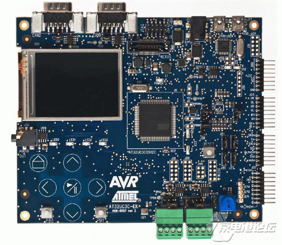
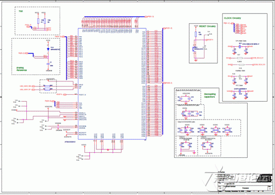
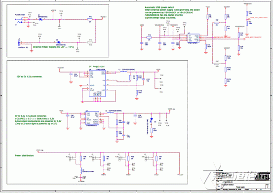
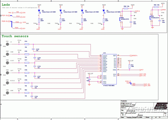
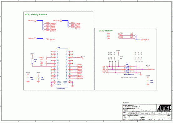
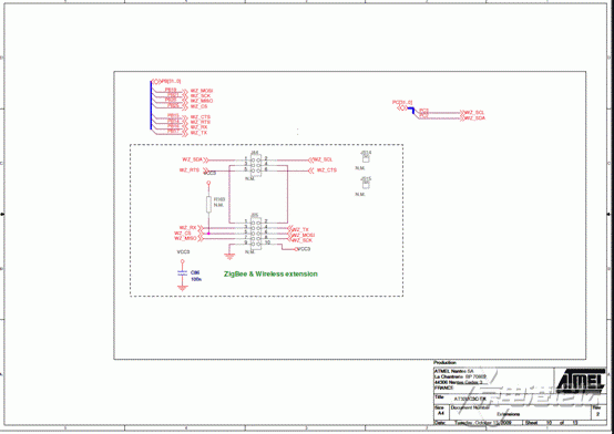
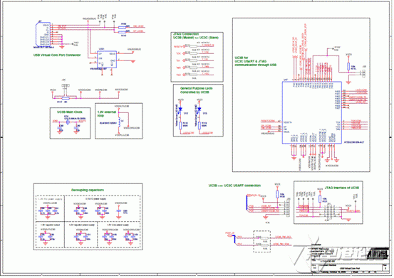
AT32UC3C-EK评估板 The Atmel® AT32UC3C-EK is an evaluation kit and development system for the Atmel AVR® UC3 AT32UC3C0512C microcontroller. As a development system, the board notably provides on-board memory, a USB communication interface, CAN and LIN network interfaces and the JTAG programming and debugging interface. The AT32UC3C-EK also features expansion headers; one of these is the wireless expansion header (named WLESS header on the PCB线路板). AT32UC3C-EK评估板主要特点: • Kit Features Overview • Kit Content • Hardware Description • Schematic |


 热点图文
热点图文