|
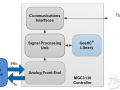
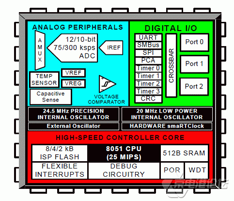
Silabs 公司的C8051F99x系列是超低功耗容性触摸传感的全集成混淆信号系统级芯片(SoC)MCU,具有最低的功耗和最高的触摸敏捷度,广泛适用于容性按钮,滑块,容性靠近检测等。C8051F99x系列接纳8051兼容的微控制器核,性能高达25MIPS,具有在系统全速非破坏性的调试接口和带模拟复接器的10位300ksps或12位75ksps单端ADC,以及多达8kB的闪存和512B RAM,工作电压1.8到3.6 V,主要用在仪表盘,触摸屏,游戏系统,住宅区HVAC,家用电器,玩具,传真机/打印机/扫描仪面板和工业接口等。本京电港论坛文章先容了C8051F99x-C8051F98x主要亮点和特点,方框架图和C8051F990滑块评估板主要特点与电路原理图纸。 C8051F99x-C8051F98x devices are fully integrated mixed-signal system-on-a-chip MCUs. Highlighted features are listed below. C8051F99x-C8051F98x主要亮点: Ultra low power consumption in active and sleep modes. High-speed pipelined 8051-compatible microcontroller core (up to 25 MIPS) In-system, full-speed, non-intrusive debug interface (on-chip) 10-bit 300 ksps or 12-bit 75 ksps single-ended ADC with analog multiplexer 6-bit programmable current reference (resolution can be increased with PWM) Precision programmable 24.5 MHz internal oscillator with spread spectrum technology. 8 kB , 4 kB, or 2 kB of on-chip Flash memory 512 bytes of on-chip RAM SMBus/I2C, Enhanced UART, and Enhanced SPI serial interfaces implemented in hardware Four general-purpose 16-bit timers Programmable counter/timer array (PCA) with three capture/compare modules and watchdog timer function On-chip power-on reset, VDD monitor, and temperature sensor One on-chip voltage comparator Up to 14 Capacitive Touch (QuickSense™) Inputs Up to 17 Port I/O With on-chip power-on reset, VDD monitor, watchdog timer, and clock oscillator, the C8051F99x-C8051F98x devices are truly stand-alone system-on-a-chip solutions. The Flash memory can be reprogrammed even in-circuit, providing non-volatile data storage, and also allowing field upgrades of the 8051 firmware. User software has complete control of all peripherals, and may individually shut down any or all peripherals for power savings. The on-chip Silicon Labs 2-Wire (C2) Development Interface allows non-intrusive (uses no on-chip resources), full speed, in-circuit debugging using the production MCU installed in the final application. This debug logic supports inspection and modification of memory and registers, setting breakpoints, single stepping, run and halt commands. All analog and digital peripherals are fully functional while debugging using C2. The two C2 interface pins can be shared with user functions, allowing in-system debugging without occupying package pins. Each device is specified for 1.8 to 3.6 V operation over the industrial temperature range (C40 to +85 ℃). The Port I/O and RST pins are powered from the supply voltage. The C8051F99x-C8051F98x devices are available in 20-pin or 24-pin QFN or 24-pin QSOP packages. All package options are lead-free and RoHS compliant. C8051F99x-C8051F98x主要特点: Ultra Low Power Consumption -150 μA/MHz in active mode (24.5 MHz clock) -2 μs wakeup time -10 nA sleep mode with memory retention -50 nA sleep mode with brownout detector -300 nA sleep mode with LFO -600 nA sleep mode with external crystal Supply Voltage 1.8 to 3.6 V -Built-in LDO regulator allows a high analog supply voltage and low digital core voltage -2 built-in supply monitors (brownout detector) for sleep mode and active modes 12-Bit or 10-Bit Analog to Digital Converter -±1 LSB INL (10-bit mode); ±1.5 LSB INL (12-bit mode) no missing codes -Programmable throughput up to 300 ksps (10-bit mode) or 75 ksps (12-bit mode) -Up to 10 external inputs -On-chip voltage reference; 0.5x gain allows measuring voltages up to twice the reference voltage -16-bit auto-averaging accumulator with burst mode provides increased ADC resolution -Data dependent windowed interrupt generator -Built-in temperature sensor Capacitive Sense Interface (F99x) -Supports buttons, sliders, wheels, and capacitive proximity sensing -Fast 40 μs per channel conversion time -16-bit resolution, up to 14 input channels -Auto scan and wake-on-touch -Auto-accumulate up to 64x samples Analog Comparator -Programmable hysteresis and response time -Configurable as wake-up or reset source 6-Bit Programmable Current Reference -Up to ±500 μA, can be used as a bias or for generating a custom reference voltage -PWM enhanced resolution mode High-Speed 8051 μC Core -Pipelined instruction architecture; executes 70% of instructions in 1 or 2 system clocks -Up to 25 MIPS throughput with 25 MHz clock -Expanded interrupt handler Memory -512 bytes RAM -8 kB (F990/1/6/7, F980/1/6/7), 4 kB (F982/3/8/9), or 2 kB (F985) Flash; in-system programmable Digital Peripherals -Up to 17 port I/O; high sink current and programmable drive strengthHardware SMBus™/I2C™, SPI™, and UART serial ports available concurrently -Four general purpose 16-bit counter/timers -Programmable 16-bit counter/timer array with three capture/compare modules and watchdog timer Clock Sources -Internal oscillators: 24.5 MHz, 2% accuracy supports UART operation; 20 MHz low power oscillator requires very little bias current. -External oscillator: Crystal, RC, C, or CMOS Clock -SmaRTClock oscillator: 32 kHz Crystal or internal -Can switch between clock sources on-the-fly; useful in implementing various power saving modes On-Chip Debug -On-chip debug circuitry facilitates full-speed, non-intrusive in-system debug (no emulator required) -Provides breakpoints, single stepping -Inspect/modify memory and registers -Complete development kit Packages -20-pin QFN (3 x 3 mm) -24-pin QFN (4 x 4 mm) -24-pin QSOP (easy to hand-solder) Temperature Range: C40 to +85 ℃ C8051F99x 主要应用: Instrumentation panels Touch panels Kiosks Gaming Systems Industrial interface Security Residential HVAC Home appliances Toys Keyboards Fax/printer/scanner front panels
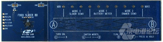
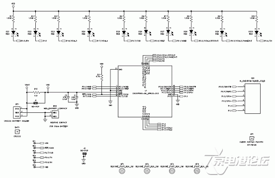
C8051F990滑块评估板 The C8051F990 Slider Evaluation Kit demonstrates the system level possibilities that can be achieved when combining Silicon Laboratories QuickSense™ technology with the C8051F99x ultra low power capacitive sensing MCU. The result is a battery powered capacitive sensing solution that has the following features: C8051F990滑块评估板主要特点: Gesture Recognition―Quicksense™ events enable the ability to detect gestures, such as a “pinch”, on the slider. In this system, the “pinch” gesture is used to switch between different demonstration modes.
|


 热点图文
热点图文