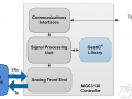
Renesas公司的RZ系列/RZA系列产物单片微控制器是{方案}ARM Cortex™-A9处理器,集成了用来系统配置的外设功能如3MB RAM,多功能计时器,OS计时器,实时时钟,带FIFO的串行通信接口,I2C总线接口,媒体当地总线,SPDIF接口,CD-ROM译码器,ADC,LIN接口,以太网控制器,视频显示控制器等.别的还集成了32KB L1指令缓存,32KB L1数据缓存和128KB L2缓存.CPU最大工作频率高达400MHz,主要用在家用电器,工业设备,修建物管理,电网和交通等.本京电港论坛文章先容了RZ/A1L系列主要特点, CPU板RTK772100BC00000BR系统配置框架图和主要特点,框架图以及所用IC和毗连主要元件表和PCB线路板结构图,详细电路原理图纸.
This LSI is a single-chip microcontroller that includes an ARM Cortex™-A9 processor along with the integrated peripheral functions requi ed to configure a system.
This LSI includes a 32-Kbyte L1 instruction cache, a 32-Kbyte L1 data cache, and a 128-Kbyte L2 cache. This LSI also includes on-chip peripheral functions necessary for system configuration, such as a 3-Mbyte large capacity RAM (128 Kbytes are shared by the data-retention RAM), data-retention RAM, multi-function timer pulse unit 2, OS timer, realtime clock, serial communication interface with FIFO, serial communication interface, I 2C bus interface, serial sound interface, media local bus, SCUX, CAN interface, IEBus™* controller, Renesas SPDIF interface, Renesas serial peripheral interface, SPI multi I/O bus controller, CD-ROM decoder, A/D converter, LIN interface, Ethernet controller, USB 2.0 host/function, video display controller 5, capture engine unit, SD host interface, MMC host interface, interrupt controller modules, and general I/O ports
RZ/A1L系列主要特点:
CPU
ARM Cortex-A9 processor
Maximum operating frequency: 400 MHz
Instruction cache size: 32 Kbytes
Data cache size: 32 Kbytes
TLB entries: 128 entries
Jazelle architecture extension: Full implementation
Media processing engine with NEON technology
L2 cache memory
ARM CoreLink™ Level 2 Cache Controller L2C-310
Operating frequency: 133 MHz
Cache size: 128 Kbytes
Interrupt controller
ARM PrimeCell® Generic Interrupt Controller (PL390)
External interrupt pins (NMI, IRQ7 to IRQ0, and TINT121 to TINT0)
On-chip peripheral interrupts: Priority level set for each module
32 priority levels available
Bus state controller
Address space divided into six areas (0 to 5), each a maximum of 64 Mbytes
The following features settable for each area independently
―Bus size (8, 16, or 32 bits): Available sizes depend on the area.
―Number of access wait cycles (different wait cycles can be specified for read and write access cycles in some areas)
―Idle wait cycle insertion (between the same area access cycles or different area access cycles)
―Specifying the memory to be connected to each area enables direct connection to SRAM, SRAM with byte selection, SDRAM, and burst ROM (clocked synchronous or asynchronous). The address/data multiplexed I/O (MPX) interface is also available.
Outputs a chip select signal (CS0 to CS5) according to the target area (CS assert or negate timing can be selected by software)
SDRAM refresh
Auto refresh or self refresh mode selectable
SDRAM burst access
Direct memory access controller
Sixteen channels; external requests are available for one of them.
Can be activated by on-chip peripheral modules.
A specific DMA transfer interval can be specified to adjust the bus occupancy.
Link mode (DMA transfer under descriptor control) supported
Transfer information can be automatically reloaded.
Clock pulse generator
Clock mode: Input clock can be selected from external input (EXTAL or USB_X1) or crystal resonator.
Input clock can be multiplied by 32 (max.) by the internal PLL circuit.
Peak values of EMI noise can be reduced by the on-chip SSCG circuit.
Five types of clocks generated:
―CPU clock (Iφ): Maximum 400.00 MHz
―Internal bus clock (Bφ): Maximum 133.33 MHz
―Peripheral clock 1 (P1φ): Maximum 66.67 MHz
―Peripheral clock 0 (P0φ): Maximum 33.33 MHz
Watchdog timer
On-chip one-channel watchdog timer
A counter overflow can reset the LSI.
Power-down modes
Four power-down modes provided to reduce the power consumption in this LSI
―Sleep mode
―Software standby mode
―Deep standby mode
―Module standby mode
Multi-function timer pulse unit 2
Maximum 16 lines of pulse inputs/outputs based on five channels of 16-bit timers
18 output compare and input capture registers
Input capture function
Pulse output modes
Toggle, PWM, complementary PWM, and reset-synchronized PWM modes
Synchronization of multiple counters
Complementary PWM output mode
―Non-overlapping waveforms output for 3-phase inverter control
―Automatic dead time setting
―0% to 100% PWM duty value specifiable
―A/D converter start request delaying function
―Interrupt skipping at crest or trough
Reset-synchronized PWM mode
Three-phase PWM waveforms in positive and negative phases can be output with a required duty value.
Phase counting mode
Two-phase encoder pulse counting available
OS timer
Two-channel 32-bit counters
Two operating modes:
―Interval timer mode
―Free-running comparison mode
DMA transfer request or interrupt request can be issued when a compare match occurs.
Realtime clock
Internal clock, calendar function, alarm function
Interrupts can be generated at intervals of 1/64 s by the 32.768-kHz on-chip crystal oscillator.
Serial communication interface with FIFO
Five channels
Clock synchronous mode or asynchronous mode selectable
Simultaneous transmission and reception (full-duplex communication) supported
Dedicated baud rate generator
Separate 16-byte FIFO registers for transmission and reception
Modem control function (channels 0 to 2 in asynchronous mode)
Serial communication interface
Two channels
Clock synchronous mode, asynchronous mode, or smart card interface mode is selectable.
Simultaneous transmission and reception (full-duplex communication) supported
Dedicated baud rate generator
LSB first/MSB first selectable
Modem control function
Encoding and decoding of IrDA communications waveforms in accord with version 1.0 of the IrDA standard (on channel 0)
Renesas serial peripheral interface
Three channels
SPI operation
Master mode and slave mode selectable
Programmable bit length, clock polarity, and clock phase can be selected.
Consecutive transfers
MSB first/LSB first selectable
Maximum transfer rate: 33.33 Mbps
SPI multi I/O bus controller
One channel
Up to two serial flash memories with multiple I/O bus sizes (single/dual/quad) can be connected.
External address space read mode (built-in read cache)
SPI operating mode
Clock polarity and clock phase can be selected.
MSB first/LSB first selectable
Maximum transfer rate: 533.33 Mbps (with two serial flash memories connected)
I2C bus interface
Four channels
Master mode and slave mode supported
Support for 7-bit and 10-bit slave address formats
Support for multi-master operation
Timeout detection
Serial sound interface
Four-channel bidirectional serial transfer
Duplex communication (channels 0, 1, and 3)
Support of various serial audio formats
Support of master and slave functions
Generation of programmable word clock and bit clock
Multi-channel formats
Support of 8, 16, 18, 20, 22, 24, and 32-bit data formats
Support of eight-stage FIFO for transmission and reception
Support of TDM mode
Support of WS continue mode in which the SSIWS signal is not stopped.
Support of direct transfer to the SCUX module
A change of the sampling frequency can be detected.
Media local bus
MediaLB (OS62400 manufactured by SMSC) for connection with the INIC incorporated.
Conforms with version 2.0 of the MediaLB standard. Data transfer at up to 50 Mbps is possible.
SCUX Sampling rate conversion
―Asynchronous or synchronous sampling rate conversion is possible.
―Sampling rate (synchronous mode)
Note: The selectable sampling rates depend on the number of used channels and rate ratio.
Input [kHz]: 8, 11.025, 12, 16, 22.05, 24, 32, 44.1, 48, 64, 88.2, or 96 is selectable.
Output [kHz]: 8, 16, 24, 44.1, 48, or 96 is selectable.
―Sampling rate (asynchronous mode)
Note: The selectable sampling rates depend on the number of used channels and rate ratio.
Input/output [kHz]: 1 to 96
―Data format: 16 or 24 bits
Digital volume and mute functions
―The digital volume can be set within the range from a multiple of 0 to 8 (−120 to 18 dB)
―Volume ramping supports soft mute, fade-in, and fade-out.
―The zero crossing mute function can apply muting at zero-crossing points.
Mixer
―Data of two to four source systems can be mixed (added together) into one system.
―The ratio to add the sources can be set.
Direct transfer to the serial sound interface module is supported.
CAN interface
Two channels
ISO11898-1 compliant
Message buffer:
―Up to 64 2-channel receive message buffers: shared among all channels.
―16 transmit message buffers per channel
IEBusTM controller
Conforms with the IEBus protocol (communication modes 1 and 2).
Transfer rates: approximately 17 kbps (in communication mode 1),approximately 26 kbps (in communication mode 2)
Maximum numbers of bytes for transfer: 32 bytes/frame (in communication mode 1),128 bytes/frame (in communication mode 2)
Operating clock: 8 MHz
Note: Input of peripheral clock 0 (P0φ) running at 32 MHz is required.
Renesas SPDIF interface
Support of IEC60958 standard (stereo and consumer use modes only)
Sampling frequencies of 32 kHz, 44.1 kHz, and 48 kHz
Audio word sizes of 16 to 24 bits per sample
Biphase mark encoding
Double buffered data
Parity encoded serial data
Simultaneous transmit and receive
Receiver autodetects IEC 61937 compressed mode data
CD-ROM decoder
Support of five formats: Mode 0, mode 1, mode 2, mode 2 form 1, and mode 2 form 2
Sync codes detection and protection
(Protection: When a sync code is not detected, it is automatically inserted.)
Descrambling
ECC correction
―P, Q, PQ, and QP correction
―PQ or QP correction can be repeated up to three times.
EDC check
Performed before and after ECC
Mode and form are automatically detected.
Link sectors are automatically detected.
Buffering data control
Buffering CD-ROM data including Sync code is transferred in specified format, after the data is descrambled, corrected by ECC, and checked by EDC.
LIN interface
Conforms with revisions 1.3, 2.0, 2.1, and 2.2 of the LIN protocol and SAEJ 2062.
Master mode and slave mode selectable
Ethernet controller
Conforms with the Ethernet or the IEEE802.3 MAC (Media Access Control) layer standard
MAC function
Constructs/deconstructs data frames (frame format conforming to IEEE802.3, 2000 Edition)
Supports transfer at 10 and 100 Mbps
Supports full-duplex mode
Flow control conforming to IEEE802.3x
Supports an MII (Media Independent Interface) for connection to a PHY interface in conformance with IEEE 802.3
Upward protocol support (checksum) function
E-DMAC (Direct Memory Access Controller for Ethernet controller) function
USB 2.0 host/function module Two channels
Conforms to the Universal Serial Bus Specification Revision 2.0
480-Mbps, 12-Mbps, and 1.5-Mbps transfer rates provided (host mode)
480-Mbps and 12-Mbps transfer rates provided (function mode)
On-chip 8-Kbyte RAM as communication buffers
Video display controller 5
Video input interface
BT601, BT656 format (NTSC/PAL) input: Input clock: 27 MHz/54 MHz
Digital pin input (channel 0):
YCbCr422, YCbCr444, RGB888, RGB666, RGB565
Digital pin input size:
Maximum input video image size to be set*: 1440 pixels × 1024 lines (horizontal × vertical)
Note:*Depends on the AC characteristics of the connected device.
Examples of input video image size :
XGA (1024 × 768),
SVGA (800 × 600),
WVGA (800 × 480),
VGA (640 × 480),
WQVGA (480 × 240),
QVGA (320 × 240, 240 × 320)
Input video control
Horizontal noise reduction (NR) and brightness and gain adjustment using matrix operation
scaling control
Vertical and horizontal scaling up or down of input video possible at a desired ratio (scaling up of graphics also possible)
Scaling up ratio: 1 to 8; scaling down ratio: 1/8 to 1
Interpolation: Hold or linear selectable
2D IP conversion: 2D IP conversion through separately setting the initial phases
for the top and bottom fields
Video recording
Output pixel format: YCbCr444, YCbCr422, RGB888, RGB565
Output field rate: 1/1, 1/2, 1/4, 1/8
Rotation: Horizontal mirroring and 90/180/270 degree rotation for YCbCr422 and RGB565
Maximum video image size to be stored: ×1 size of input video image
Output video control
Black stretch: Black area stretched according to Y signal state
Enhancer capability: LTI (transient improvement) and sharpness (contour emphasis) for Y signal
Video display controller 5 Three graphics layers (one of them also for input video)
Available input pixel formats
1 bit/pixel: CLUT1
4 bits/pixel: CLUT4
8 bits/pixel: CLUT8
16 bits/pixel: YCbCr422 (graphics layers 0 and 1), RGB565, ARGB1555, RGBA5551, ARGB4444
32 bits/pixel: ARGB8888, RGBA8888, RGB888, YCbCr444 (graphics layer 0)
Superimposition
Alpha blending in a rectangular area:
Input video, layer 1, and layer 2 blended according to the transparency percentage α
(fade-in and fade-out function available)
Chroma key function:
Mixing based on transparency percentage α using the specified RGB and CLUT value
Pixel-base alpha blending:
Alpha blending for each pixel based on transparency percentage α
Panel output control
Panel output correction:
Brightness adjustment and contrast adjustment, gamma correction, panel dithering
TCON:
Various timing output for LCD panel driving provided by a total of seven vertical and horizontal
panel driver signals
Panel output pixel format: RGB888, RGB666, RGB565, serial RGB
Output video image size:
Maximum output video image size to be set*:
1999 pixels × 2035 lines (horizontal × vertical)
Note:*Depends on the AC characteristics of the display panel.
Examples of output video image size:
XGA (1024 × 768),
SVGA (800 × 600),
WVGA (800 × 480),
VGA (640 × 480),
WQVGA (480 × 240),
QVGA (320 × 240, 240 × 320)
Capture engine unit Examples of input video image size :
WXGA (1280 × 768),
XGA (1024 × 768),
SVGA (800 × 600),
WVGA (800 × 480),
VGA (640 × 480),
WQVGA (480 × 240),
QVGA (320 × 240, 240 × 320)
Note: Depends on the AC characteristics of the connected device.
Input format: 8-bit YCbCr422 binary data
Memory output format: YCbCr422, YCbCr420
Note: The captured data cannot be displayed via the video display controller 5 because the Y data
and CbCr data are split when written to memory.
SD host interface
Two channels
SD memory I/O card interface (1-/4-bit SD bus)
Error check function: CRC7 (command), CRC16 (data)
Interrupt requests
―Card access interrupt
―SDIO access interrupt
―Card detect interrupt
DMA transfer requests
―SD_BUF write
―SD_BUF read
Card detection function, write protect supported
MMC host interface
Interface to multi-media card (MMC)
Data bus: 1-/4-/8-bit MMC mode
Interrupt requests: card detection, error/time-out, and normal operation
DMA transfer requests: CE_DATA write and CE_DATA read
Card detection function
General I/O ports 176-pin QFP or BGA: 78 I/Os, 8 inputs with open-drain outputs, and 14 inputs (input only)
208-pin QFP: 100 I/O pins, 8 input pins with open-drain outputs, and 14 inputs (input only)
Input or output can be selected for each bit.
A/D converter
12-bit resolution
Eight input channels
Minimum conversion time: 5.0 μs
A/D conversion request by the external trigger or timer trigger
Debugging interface
ARM CoreSight architecture
JTAG-standard pin assignment
On-chip RAM
3-Mbyte large capacity memory for video display/recording and work (128 Kbytes are used for data retention)
128-Kbyte memory for data retention
(16 Kbytes × 2, 32 Kbytes × 1, 64 Kbytes × 1)
Boot modes
Four boot modes
Boot mode 0: Booting from memory (bus width: 16 bits) connected to CS0 area
Boot mode 1: Booting from a serial flash memory
Boot mode 2: Booting from a NAND flash memory with SD controller
Boot mode 3: Booting from a NAND flash memory with MMC controller
Power supply voltage Vcc: 1.10 to 1.26 V
PVcc: 3.0 to 3.6 V
Package
PLBG0176KA-A
176-pin BGA, 8-mm square, 0.5-mm pitch
JEITA package code: P-LFBGA176-8 × 8-0.50
RENESAS code: PLBG0176KA-A
PLQP0176KB-A
176-pin QFP, 24-mm square, 0.5-mm pitch
JEITA package code: P-LFQFP176-24 × 24-0.50
RENESAS code: PLQP0176KB-A
PLQP0208KB-A
208-pin QFP, 28-mm square, 0.5-mm pitch
JEITA package code: P-LFQFP208-28 × 28-0.50
RENESAS Code : PLQP0208KB-A
RTK772100BC00000BR is a CPU board to evaluate functions and performance of Renesas Electronics RISC microcomputer R7S72100 and to execute development and evaluation of its application software.
R7S72100 CPU板主要特点:
• The following external memories are generally included.
- NOR flash memory: 64MB×2 (16-bit bus connection)
- SDRAM: 64MB×2 (16-bit bus connection)
- Serial flash memory: 64MB×3
- EEPROM: 16KB×1
• Any of NOR flash memory, serial flash memory, SD controller on-chip NAND flash memory, and MMC controller on-chip NAND flash memory can be selected as a boot memory.
• A serial port connector (RS-232C or USB Mini-B), USB connectors, CAN connectors, SD card slot, MMC card slot,RCA connector for video input, and MOST I/F connector are generally included as the R7S72100 peripheral function interface.
• An audio CODEC is included to enable advance development of the audio system.
• The USB connectors generally include the series A receptacles. The board pattern enables the Mini-B receptacles to be implemented for the USB host/function module evaluation.
• A LAN connector is generally included to enable software development or evaluation using the Ethernet.
• Data bus, address bus and on-chip peripheral function pins of the R7S72100 are all connected to the expansion connectors to enable timing evaluation with the peripheral devices using measurement instrument, or development of expansion board for its application.
• The ARM JTAG 20 and the CoreSight 20 are mounted to connect with the R7S72100 user debug interface.
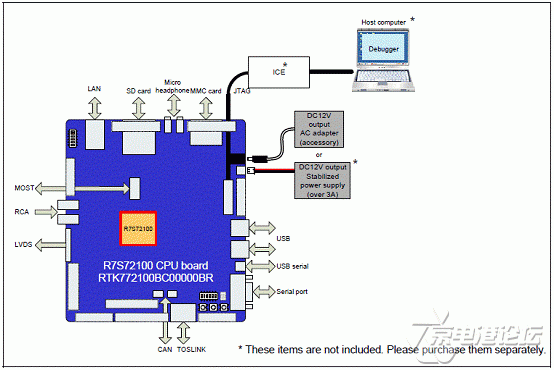
图1{京电港论坛}. R7S72100 CPU 板RTK772100BC00000BR系统配置框架图
R7S72100 CPU板RTK772100BC00000BR主要特点:


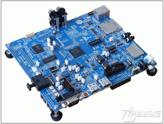
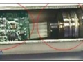
图2{京电港论坛}. R7S72100 CPU 板RTK772100BC00000BR外形实物图
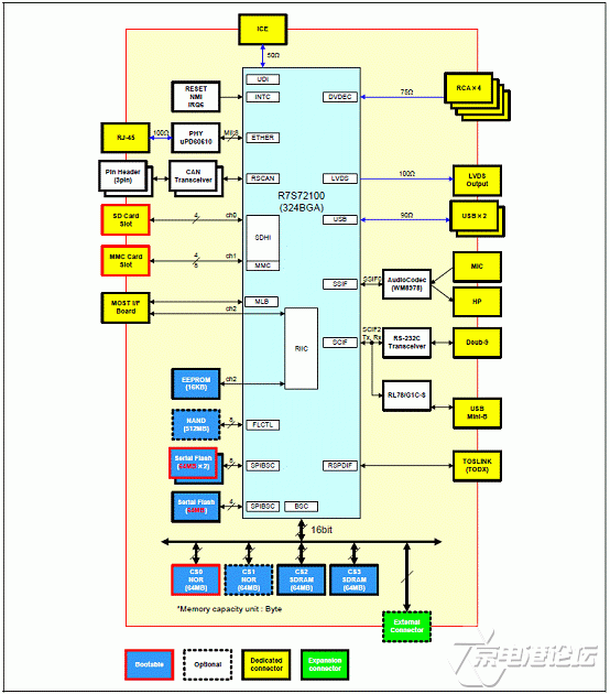
图3{京电港论坛}.RTK772100BC00000BR板框架图
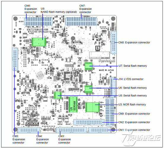
图4{京电港论坛}.RTK772100BC00000BR板PCB线路板结构图(顶层)
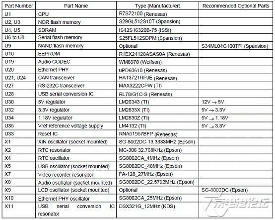
RTK772100BC00000BR板主要元件表:IC
RTK772100BC00000BR板主要元件表:毗连器
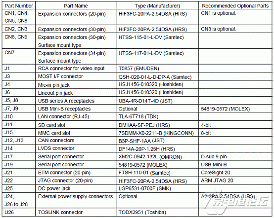
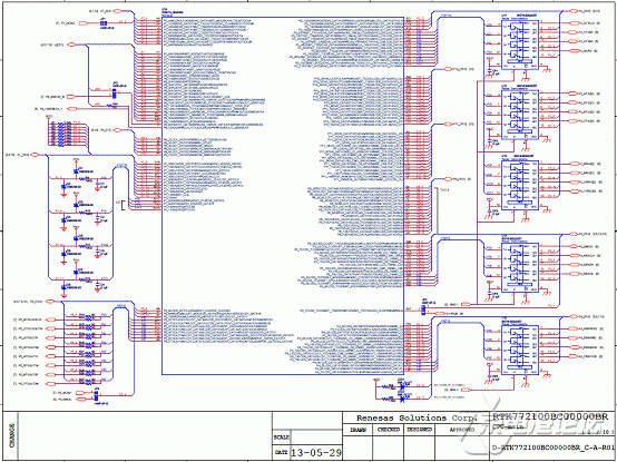
图4{京电港论坛}.RTK772100BC00000BR板电路原理图纸(1)
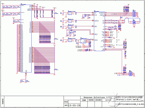
图5{京电港论坛}.RTK772100BC00000BR板电路原理图纸(2)

图4{京电港论坛}.RTK772100BC00000BR板电路原理图纸(1)
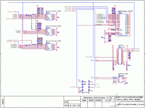
图5{京电港论坛}.RTK772100BC00000BR板电路原理图纸(2)
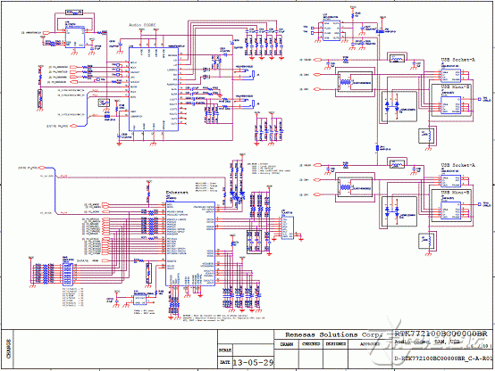
图6{京电港论坛}.RTK772100BC00000BR板电路原理图纸(3)
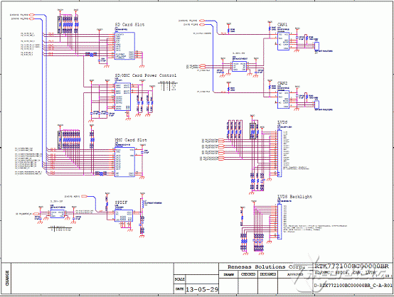
图7{京电港论坛}.RTK772100BC00000BR板电路原理图纸(4)
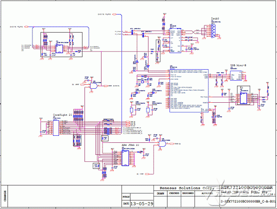
图8{京电港论坛}.RTK772100BC00000BR板电路原理图纸(5)
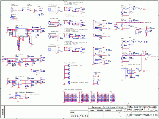
图9{京电港论坛}.RTK772100BC00000BR板电路原理图纸(6)
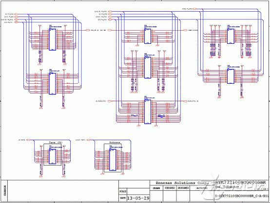
图1{京电港论坛}0.RTK772100BC00000BR板电路原理图纸(7)
详情请复制打开此衔接地址:
mcu/doc/rz/r01uh0437ej0100_rz_a1l.pdf">http://documentation.renesas.com/doc/products/mpumcu/doc/rz/r01uh0437ej0100_rz_a1l.pdf
和
http://documentation.renesas.com/doc/products/tool/doc/r20ut2596ej_r7s72100evum.pdf


 热点图文
热点图文