|
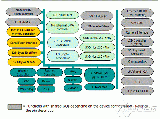
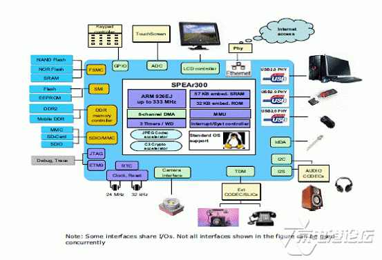
ST 公司的SPEAr300 是接纳ARM926EJ-S 核的嵌入式MPU,支持机动的存储器,具有功能强大的毗连特点和可编程的LCD接口。ARM926EJ-S 核工作频率高达333MHz,有高性能的8路DMA和动态节能特点,外接存储器LPDDR-333/DDR2-666接口,主要用在{方案}NAND闪存或NOR闪存的设备,数码相框,WiFi或IP电话,ATA PABX系统,8位或14位数码相机。本京电港论坛文章先容SPEAr300 MPU主要特别法庭性,功能方框架图,系统架构框架图以及EVALSPEAR600评估板主要特点,电路原理图纸和所用质料清单(BOM)。 The SPEAr300 is a member of the SPEAr family of embedded MPUs for networked devices. It is based on the powerful ARM926EJ-S processor (up to 333 MHz), widely used in applications where high computation performance is required. In addition, SPEAr300 has an MMU that allows virtual memory management -- making the system compliant with Linux operating system. It also offers 16 KB of data cache, 16 KB of instruction cache, JTAG and ETM (embedded trace macro-cell) for debug operations.A full set of peripherals allows the system to be used in many applications, some typical applications being HMI, Security and VoIP phones. SPEAr300主要特点: ● ARM926EJ-S 32-bit RISC CPU, up to 333 MHz C 16 Kbytes of instruction cache, 16 Kbytes of data cache C 3 instruction sets: 32-bit for high performance, 16-bit (Thumb) for efficient code density, byte Java mode (Jazelle™) for direct execution of Java code. C Tightly Coupled Memory C AMBA bus interface ● 32-KByte on-chip BootRom ● 57-KByte on-chip SRAM ● 16-bit mobile DDR/DDR2 memory controller (up to 333 MHz) ● Serial memory interface ● SDIO/MMC interface supporting SPI, SD1, SD4 and SD8 mode with card detect, write ● 8/16-bits NOR Flash/NAND Flash controller ● Boot capability from NAND Flash, serial/parallel NOR Flash, Ethernet and UART ● Boot and field upgrade capability from USB ● Multichannel DMA controller ● Color LCD Controller for STN/TFT display panels C up to 1024 x 768 resolution C 24 bpp true color ● Up to 44 GPIOs (muxed with peripheral I/Os), up to 22 with interrupt capability ● JPEG CODEC accelerator, 1 clock/pixel ● Camera interface ITU-601 with external or embedded synchronization (ITU-656 or CSI2). Picture limit is given by the line length that must be stored in a 2048 x 32 buffer ● C3 Crypto accelerator (DES/3DES/AES/SHA1) ● TDM master/slave C Up to 512 timeslots C Any input timeslot can be switched to any output timeslot, and/or can be buffered for computation C Up to 16 channels of 1 to 4 timeslots buffered during 32 ms C Up to 16 buffers can be played in output timeslots ● I2S interface, full duplex with data buffer for left and right channels allowing up to 64 ms of voice buffer (for 32 bit samples). ● 10-bit ADC, 1 Msps, 8 inputs/1-bit DAC ● 9 x 9 keyboard controller ● Ethernet MAC 10/100 Mbps (MII PHY interface) ● Two USB2.0 host (high-full-low speed) with integrated PHY transceiver ● One USB2.0 device (high-full-low speed) with integrated PHY transceiver ● SPI master/slave (Motorola, Texas instruments, National semiconductor protocols) up to 50 Mbps ● I2C (slow- fast-high speed, up to 1.2 Mb/s) master/slave ● I/O peripherals C UART (speed rate up to 460.8 kbps) C IrDA (FIR/MIR/SIR) 9.6 kbps to 4 Mbps speed-rate ● Advanced power saving features C Normal, Slow, Doze and Sleep modes CPU clock with software-programmable frequency C Enhanced dynamic power-domain management Clock gating functionality C Low frequency operating mode C Automatic power saving controlled from application activity demands ● Vectored interrupt controller ● System and peripheral controller C 3 pairs of 16-bit general purpose timers with programmable prescaler. C RTC with separate power supply allowing battery connection C Watchdog timer C Miscellaneous registers array for embedded MPU configuration ● Programmable PLL for CPU and system clocks ● JTAG IEEE 1149.1 boundary scan ● ETM9 interface and embedded ICE-RT ● ETM functionality multiplexed on primary pins ● Supply voltages C 1.2 V core, 1.8 V to 3.3 V I/Os ● Operating temperature: - 40 to 85℃ ● LFBGA289 (15 x15 mm, pitch 0.8 mm) SPEAr300应用: ■ SPEAr300 embedded MPU is configurable in 13 sets of peripheral functions targeting a range of applications: C General purpose NAND Flash or NOR Flash based devices C Digital photo frames WiFi or IP phones (low end or high end) C ATA PABX systems (with or without I2S)| 8-bit or 14-bit camera (with or without LCD)
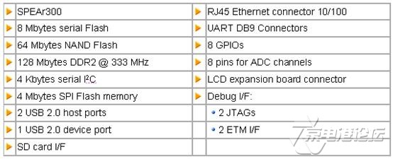
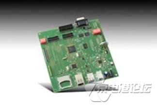
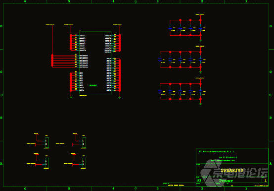
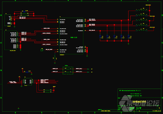
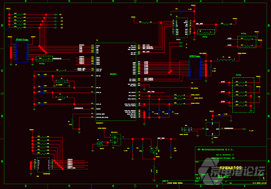
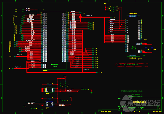
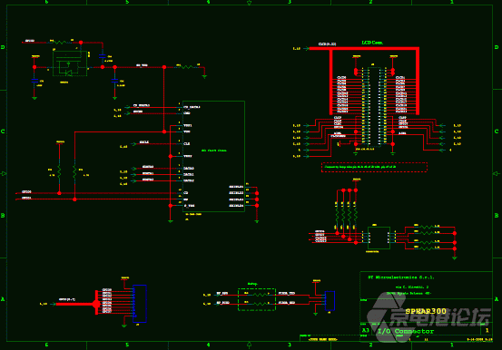
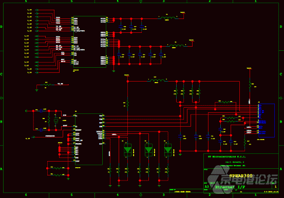
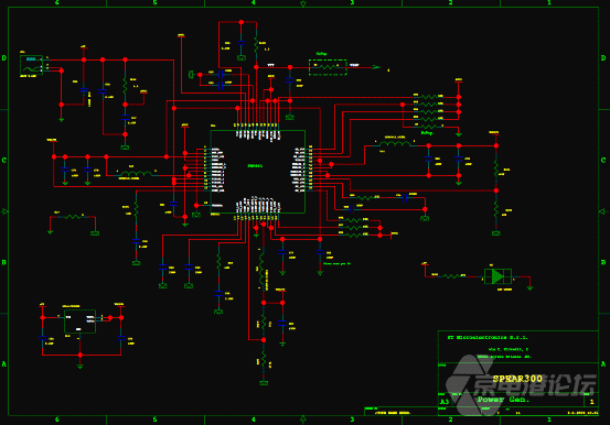
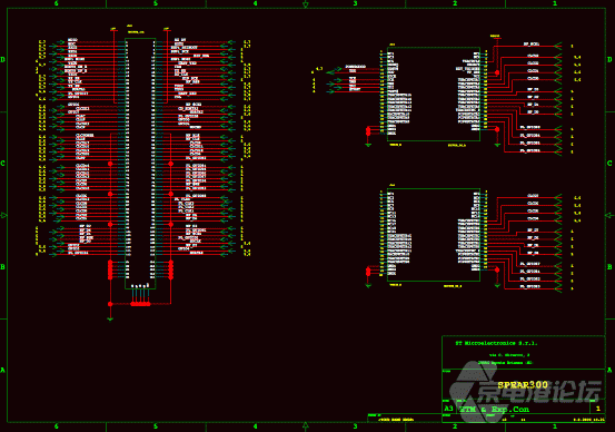
EVALSPEAR300评估板 The EVALSPEAR300 evaluation board is a complete development platform for SPEAr300. It offers an easy and flexible solution for demonstrating device capabilities and quickly evaluating features and peripherals. It integrates a SPEAr300 embedded MPU with a high-performance ARM 926EJ-S core, two USB 2.0 hosts, one USB 2.0 device port and Ethernet MAC. The evaluation boards include a complete range of hardware features for evaluating SPEAr300 performance and for starting development of a wide range of applications. Features include serial and parallel Flash, DDR2 memory, USB 2.0, fast Ethernet, SPI, Fast IrDA, I2C, UART port SD card interface and LCD expansion board connector. The board features an industry-standard JTAG and ETM connectors allowing developers to choose from a wide choice of development tools. EVALSPEAR300评估板包罗:
EVALSPEAR300评估板质料清单(BOM):
详情请复制打开此衔接地址: |


 EVALSPEAR300评估板质料清单.xls


 热点图文
热点图文