Silabs公司的Si5386是高性能12路任意频率无线抖动衰减时钟发生器,采用第四代DSPLL技术,差分输入频率7.68 MHz - 750 MHz, LVCMOS输入频率7.68 MHz- 250 MHz,差分输出频率(整数)高达2.94912 GHz,支持JESD204B.分数输出频率:差分高达735MHz,LVCMOS高达250MHz. 12 kHzC20 MHz的抖动80fs,输出格式可配置为LVDS, LVPECL,LVCMOS, CML和HCSL,输出信号幅度200 - 3200 mV,主要用在云无线接入网络PRH,小型基站,无线基站,有源天线系统,分布式天线系统等.本文介绍了Si5386 Rev. E和Si5386主要特性,框图,应用框图以及评估板Si5386E-E-EB主要特性,框图,电路图,材料清单和PCB设计图.
The Si5386 is a high performance, integer and fractional clock generator for wireless applications which demand the highest level of integration and phase noise performance. Based on Silicon Laboratories ’4th generation DSPLL technology, the Si5386combines frequency synthesis and jitter attenuation in a highly integrated digital solutionthat eliminates the need for external VCXO and loop filter components. A fixedfrequency crystal that provides frequency stability for free-run and holdover modes isintegrated within the package saving valuable PCB space. This all-digital solutionprovides superior performance that is highly immune to external board disturbancessuch as power supply noise.
Modern C-RAN remote radio heads and fixed wireless systems require a diverse setof clocks such as ADC/DAC, RF LOs, eCPRI/CPRI, and Ethernet clocks. TheSi5386 architecture is designed to deliver high-performance JESD204B DCLK andSYSREF clock pairs and flexible any-rate clocks for non-LTE clocks such as Ethernetand system reference clocks all from a single IC.
The Si5386 ’s internal DSPLL provides jitter attenuation and any-frequency multiplication of the selected input frequency without theneed for external VCXOs or loop filters. Input switching is controlled manually or automatically using an internal state machine. The oscillator circuit (OSC) provides a frequency reference which determines output frequency stability and accuracy while the device is infree-run or holdover mode using the integrated crystal provided inside the Si5386 package. The integrated crystal is not only convenient,but saves valuable PCB area. The high-performance MultiSynthdividers (N) generate integer or fractionally related output frequenciesfor the output stage. A crosspoint switch connects any of the MultiSynth generated frequencies to any of the outputs. Additional integer division (R) determines the final output frequency. Further, the DSPLL is specially calibrated for ultra-low phase noise whenconfigured for LTE frequencies with JESD204B outputs. This integration provides a clock-tree-on-a-chip solution for applications thatneed a mix of 4G/LTE and general-purpose frequencies.
Si5386 Rev. E主要特性:
• Flexible timing in a single IC
• Generates any combination of output frequencies from anyinput frequency
• Input frequency range:
• Differential: 7.68 MHz to 750 MHz
• LVCMOS: 7.68 MHz to 250 MHz
• Output frequency range (Integer):
• Differential: up to 2.94912 GHz with JESD204B support
• Output frequency range (fractional):
• Differential: up to 735 MHz
• LVCMOS: up to 250 MHz
• Ultra-low jitter: 80 fs typ(12 kHzC20 MHz)
• Programmable jitter attenuation bandwidth from 1 Hz to 4 kHz
• Highly configurable outputs compatible with LVDS, LVPECL,LVCMOS, CML, and HCSL with programmable signal amplitudefrom 200 - 3200 mV
• Status monitoring (LOS, OOF, LOL)
• Pin controlled input switching
• DSPLL with special wireless calibration
• Optional zero delay mode
• Hitless input clock switching: automatic or manual
• Automatic free-run and holdover modes
• Fastlock feature
• Glitchless on the fly output frequency changes
• Core voltage:
• VDD: 1.8 V ±5%
• VDDA: 3.3 V ±5%
• Independent output clock supply pins: 3.3 V, 2.5 V, or 1.8 V
• Output-output skew: 20 pstyp
• Serial interface: I2C or SPI
• In-circuit programmable with non-volatile OTP memory
• ClockBuilderProTM software simplifies device configuration
• Temperature range: C40 to +85 ℃
Si5386主要特性:
• Flexible timing in a single IC
• Generates any combination of outputfrequencies from any input frequency
• Input frequency range:
• Differential: 7.68 MHz to 750 MHz
• LVCMOS: 7.68 MHz to 250 MHz
• Output frequency range (Integer):
• Differential: up to 3 GHz
• Output frequency range (fractional):
• Differential: up to 735 MHz
• LVCMOS: up to 250 MHz
• Ultra-low jitter:
• 80 fs typ(12 kHzC20 MHz)
Si5386应用:
• Cloud Radio Access Network RRHs
• Small cells
• Fixed wireless
• Wireless base stations
• Active antenna systems
• Distributed antenna systems
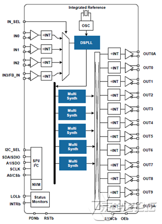
图1.Si5386框图
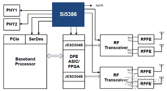
图2.Si5386应用框图
评估板Si5386E-E-EB
The Si5386E-E-EB is used for evaluating the Ultra Low Jitter, Any-Frequency, 12-output JESD204B Clock Generator. The Si5386employs fourth-generation DSPLL technology to enable clock generationfor LTE/ JESD204B applications which require the highestlevel of jitter performance. The Si5386E-E-EB has four independentinput clocks and a total of 12 outputs. The Si5386E-E-EB canbe easily controlled and configured using Silicon Labs ’ ClockBuilder Pro™ (CBPro™) software tool.
评估板Si5386E-E-EB主要特性:
• Powered from USB port or external powersupply
• Internal 48.0231 MHz crystal providesholdover mode of operation on the Si5386
• CBPro™ GUI programmable VDDOsupplies allow each of the ten primaryoutputs to have its own supply voltageselectable from 3.3, 2.5, or 1.8 V
• CBPro™ GUI-controlled voltage, current,and power measurements of VDD, VDDA,and all VDDO supplies
• Status LEDs for power supplies andcontrol/status signals of Si5386
• SMA connectors for input clocks, outputclocks and optional external timingreference clock
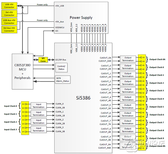
图3.评估板Si5386E-E-EB外形图

图4.评估板Si5386E-E-EB框图
图5.评估板Si5386E-E-EB电路图(1)
图6.评估板Si5386E-E-EB电路图(2)

图7.评估板Si5386E-E-EB电路图(3)
图8.评估板Si5386E-E-EB电路图(4)

图9.评估板Si5386E-E-EB电路图(5)
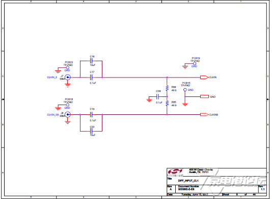
图10.评估板Si5386E-E-EB电路图(6)

图11.评估板Si5386E-E-EB电路图(7)

图12.评估板Si5386E-E-EB电路图(8)
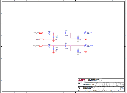
图13.评估板Si5386E-E-EB电路图(9)
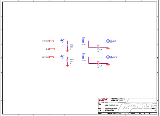
图14.评估板Si5386E-E-EB电路图(10)

图15.评估板Si5386E-E-EB电路图(11)

图16.评估板Si5386E-E-EB电路图(12)

图17.评估板Si5386E-E-EB电路图(13)

图18.评估板Si5386E-E-EB电路图(14)

图19.评估板Si5386E-E-EB电路图(15)
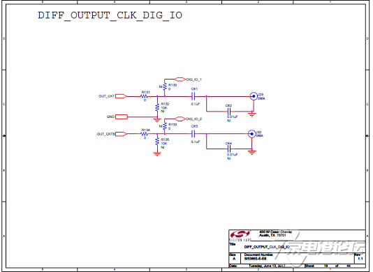
图20.评估板Si5386E-E-EB电路图(16)

图21.评估板Si5386E-E-EB电路图(17)
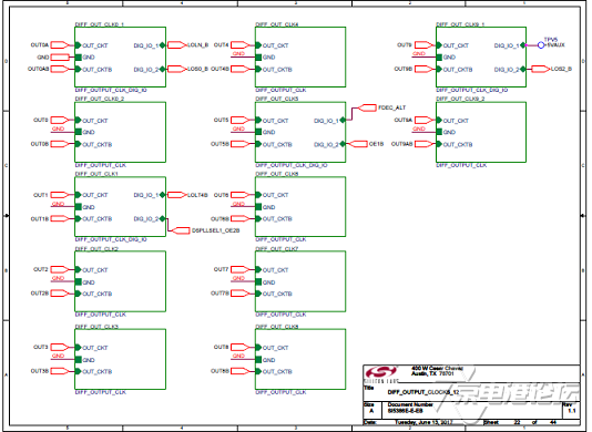
图22.评估板Si5386E-E-EB电路图(18)
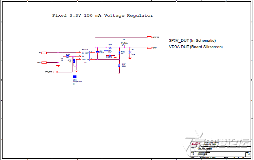
图23.评估板Si5386E-E-EB电路图(19)
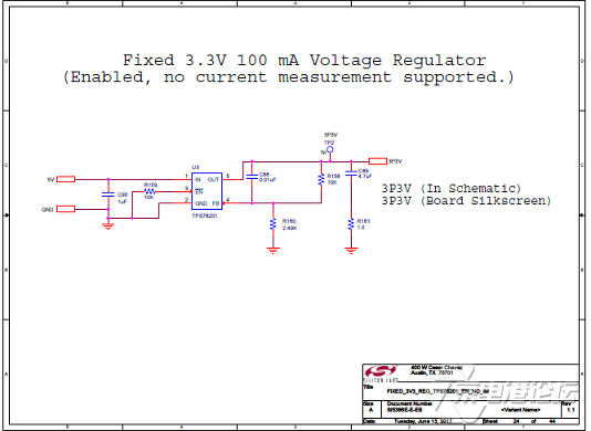
图24.评估板Si5386E-E-EB电路图(20)
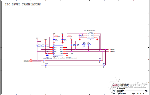
图25.评估板Si5386E-E-EB电路图(21)
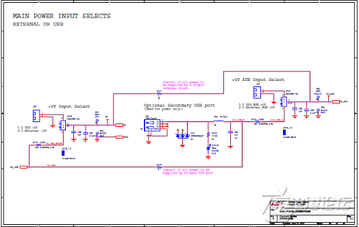
图26.评估板Si5386E-E-EB电路图(22)
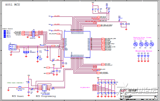
图27.评估板Si5386E-E-EB电路图(23)
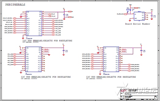
图28.评估板Si5386E-E-EB电路图(24)
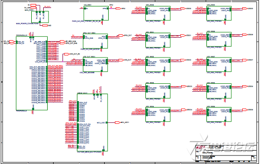
图29.评估板Si5386E-E-EB电路图(25)
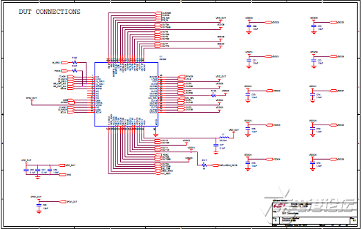
图30.评估板Si5386E-E-EB电路图(26)
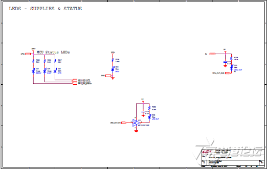
图31.评估板Si5386E-E-EB电路图(27)

图32.评估板Si5386E-E-EB电路图(28)

图33.评估板Si5386E-E-EB电路图(29)
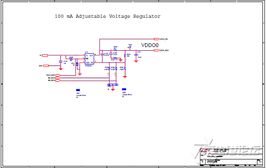
图34.评估板Si5386E-E-EB电路图(30)

图35.评估板Si5386E-E-EB电路图(31)

图36.评估板Si5386E-E-EB电路图(32)
图37.评估板Si5386E-E-EB电路图(33)

图38.评估板Si5386E-E-EB电路图(34)

图39.评估板Si5386E-E-EB电路图(35)

图40.评估板Si5386E-E-EB电路图(36)
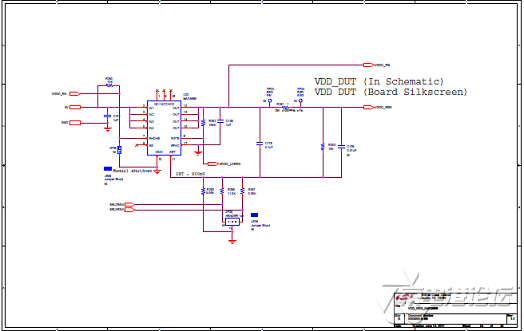
图41.评估板Si5386E-E-EB电路图(37)
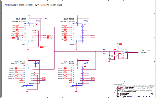
图42.评估板Si5386E-E-EB电路图(38)
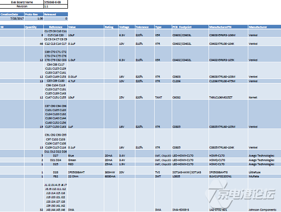
图43.评估板Si5386E-E-EB电路图(39)
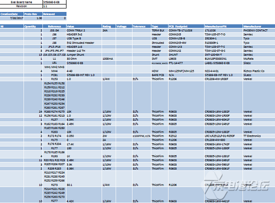
图44.评估板Si5386E-E-EB电路图(40)
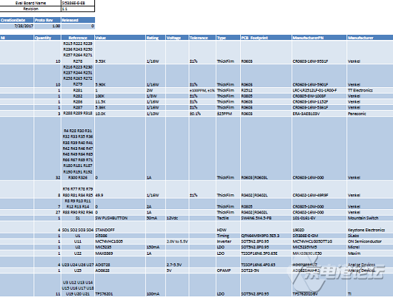
图45.评估板Si5386E-E-EB电路图(41)
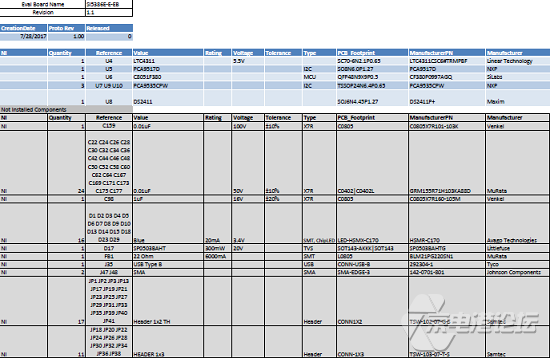
图46.评估板Si5386E-E-EB电路图(42)
评估板Si5386E-E-EB材料清单:
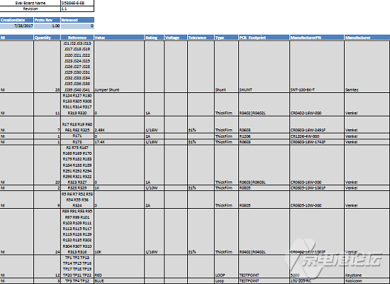
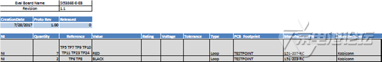
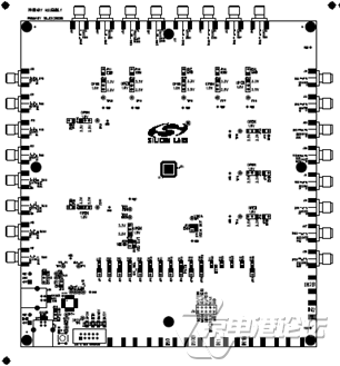
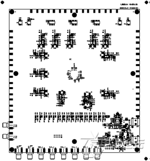
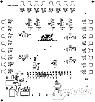

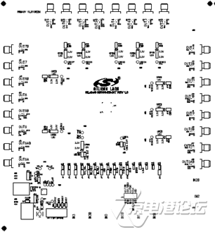
图47.评估板Si5386E-E-EB PCB设计图(1)
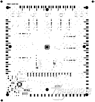
图48.评估板Si5386E-E-EB PCB设计图(2)
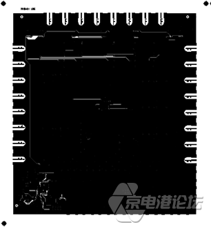
图49.评估板Si5386E-E-EB PCB设计图(3)
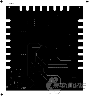
图50.评估板Si5386E-E-EB PCB设计图(4)
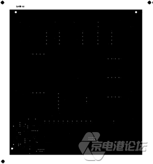
图51.评估板Si5386E-E-EB PCB设计图(5)
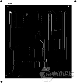
图52.评估板Si5386E-E-EB PCB设计图(6)
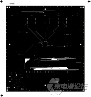
图53.评估板Si5386E-E-EB PCB设计图(7)

图54.评估板Si5386E-E-EB PCB设计图(8)
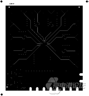
图55.评估板Si5386E-E-EB PCB设计图(9)
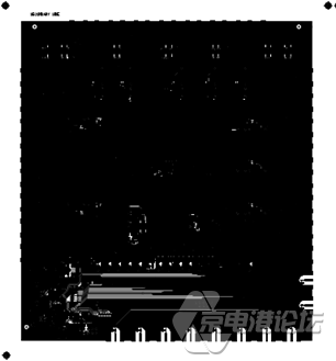
图56.评估板Si5386E-E-EB PCB设计图(10)
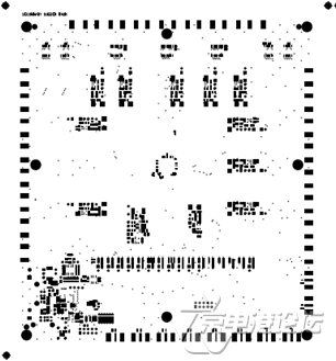
图57.评估板Si5386E-E-EB PCB设计图(11)
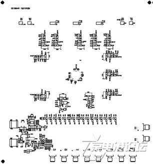
图58.评估板Si5386E-E-EB PCB设计图(12)
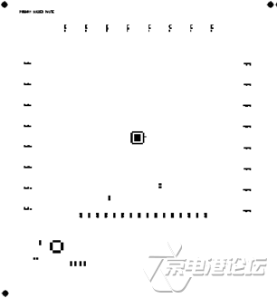
图59.评估板Si5386E-E-EB PCB设计图(13)

图60.评估板Si5386E-E-EB PCB设计图(14)
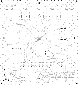
图61.评估板Si5386E-E-EB PCB设计图(15)

图62.评估板Si5386E-E-EB PCB设计图(16)

图63.评估板Si5386E-E-EB PCB设计图(17)
![]()
图64.评估板Si5386E-E-EB PCB设计图(18)
![]()
图65.评估板Si5386E-E-EB PCB设计图(19)
![]()
图66.评估板Si5386E-E-EB PCB设计图(20)
详情请见:


声明:京电港论坛转载作品均尽可能注明出处,该作品所有人的一切权利均不因本站而转移。
作者如不同意转载,既请通知本站予以删除或改正。转载的作品可能在标题或内容上或许有所改动。


 热点图文
热点图文