ST公司的STM32F777xx,STM32F778Ax和STM32F779xx系列是{方案}高性能ARM® Cortex®-M7 32位RISC核的MCU,工作频率高达216MHz,具有浮点单位(FPU)特点,支持ARM双精度和单精度数据处理指令和数据范例,集成了高达2MB闪存,512KB SRAM,16KB TCM RAM,4KB备份SRAM以及各种外设和增强I/O,主要用在马达驱动和应用控制,医疗设备,工业应用如PLC,逆变器,电路中断器,打印机和扫描仪,告警系统,视频互连和HVAC,家庭音频设备,移动应用和物联网(IoT),可穿着设备如智能手表等.本京电港论坛文章先容了STM32F779NI主要特点和框架图,以及评估板STM32F779I-EVAL主要特点,硬件框架图,电路原理图纸,质料清单和PCB线路板元件结构图.
The STM32F777xx, STM32F778Ax and STM32F779xx devices are based on the high-performance ARM® Cortex®-M7 32-bit RISC core operating at up to 216 MHz frequency. The Cortex®-M7 core features a floating point unit (FPU) which supports ARM® double-precision and single-precision data-processing instructions and data types. It also implements a full set of DSP instructions and a memory protection unit (MPU) which enhances the application security.
The STM32F777xx, STM32F778Ax and STM32F779xx devices incorporate high-speed embedded memories with a Flash memory up to 2 Mbytes, 512 Kbytes of SRAM (including 128 Kbytes of Data TCM RAM for critical real-time data), 16 Kbytes of instruction TCM RAM (for critical real-time routines), 4 Kbytes of backup SRAM available in the lowest power modes, and an extensive range of enhanced I/Os and peripherals connected to two APB buses, two AHB buses, a 32-bit multi-AHB bus matrix and a multi layer AXI interconnect supporting internal and external memories access.
All the devices offer three 12-bit ADCs, two DACs, a low-power RTC, twelve general-purpose 16-bit timers including two PWM timers for motor control, two general-purpose 32-bit timers, a true random number generator (RNG), and a cryptographic acceleration cell. They also feature standard and advanced communication interfaces.
Advanced peripherals include two SDMMC interfaces, a flexible memory control (FMC) interface, a Quad-SPI Flash memory interface, a camera interface for CMOS sensors and a cryptographic acceleration cell. Refer to Table 2: STM32F777xx, STM32F778Ax and STM32F779xx features and peripheral counts for the list of peripherals available on each part number.
The STM32F777xx, STM32F778Ax and STM32F779xx devices operate in the C40 to +105 °C temperature range from a 1.7 to 3.6 V power supply. Dedicated supply inputs for USB (OTG_FS and OTG_HS) and SDMMC2 (clock, command and 4-bit data) are available on all the packages except LQFP100 for a greater power supply choice.
• Up to four I2Cs
• Six SPIs, three I2Ss in half-duplex mode. To achieve audio class accuracy, the I2S peripherals can be clocked via a dedicated internal audio PLL or via an external clock to allow synchronization.
• Four USARTs plus four UARTs
• An USB OTG full-speed and a USB OTG high-speed with full-speed capability (with the ULPI)
• Three CANs
• Two SAI serial audio interfaces
• Two SDMMC host interfaces
• Ethernet and camera interfaces
• LCD-TFT display controller
• Chrom-ART Accelerator™
• SPDIFRX interface
• HDMI-CEC
The supply voltage can drop to 1.7 V with the use of an external power supply supervisor (refer to Section 2.18.2: Internal reset OFF). A comprehensive set of power-saving mode allows the design of low-power applications.
The STM32F777xx, STM32F778Ax and STM32F779xx devices offer devices in 10 packages ranging from 100 pins to 216 pins. The set of included peripherals changes with the device chosen.
These features make the STM32F777xx, STM32F778Ax and STM32F779xx microcontrollers suitable for a wide range of applications:
• Motor drive and application control
• Medical equipment
• Industrial applications: PLC, inverters, circuit breakers
• Printers, and scanners
• Alarm systems, video intercom, and HVAC
• Home audio appliances
• Mobile applications, Internet of Things
• Wearable devices: smartwatches.
STM32F779NI主要特点:
• Core: ARM® 32-bit Cortex®-M7 CPU with DPFPU, ART Accelerator™ and L1-cache: 16 Kbytes I/D cache, allowing 0-wait state execution from embedded Flash and external memories, up to 216 MHz, MPU, 462 DMIPS/2.14 DMIPS/MHz (Dhrystone 2.1), and DSP instructions.
• Memories
C Up to 2 Mbytes of Flash memory organized into two banks allowing read-while-write
C S RAM: 512 Kbytes (including 128 Kbytes of data TCM RAM for critical real-time data) + 16 Kbytes of instruction TCM RAM (for critical real-time routines) + 4 Kbytes of backup SRAM
C Flexible external memory controller with up to 32-bit data bus: SRAM, PSRAM, SDRAM/LPSDR SDRAM, NOR/NAND memories
• Dual mode Quad-SPI
• Graphics
C Chrom-ART Accelerator™ (DMA2D), graphical hardware accelerator enabling enhanced graphical user interface
C Hardware JPEG codec
C LCD-TFT controller supporting up to XGA resolution
C MIPI® DSI host controller supporting up to 720p 30 Hz resolution
• Clock, reset and supply management
C 1 .7 V to 3.6 V application supply and I/Os
C POR, PDR, PVD and BOR C Dedicated USB power
C 4 -to-26 MHz crystal oscillator
C I nternal 16 MHz factory-trimmed RC (1% accuracy)
C 3 2 kHz oscillator for RTC with calibration
C I nternal 32 kHz RC with calibration
• Low-power
C Sleep, Stop and Standby modes
C VBAT supply for RTC, 32×32 bit backup registers + 4 Kbytes backup SRAM
• 3×12-bit, 2.4 MSPS ADC: up to 24 channels
• Digital filters for sigma delta modulator (DFSDM), 8 channels / 4 filters
• 2×12-bit D/A converters
• General-purpose DMA: 16-stream DMA controller with FIFOs and burst support
• Up to 18 timers: up to thirteen 16-bit (1x low-power 16-bit timer available in Stop mode) and two 32-bit timers, each with up to 4 IC/OC/PWM or pulse counter and quadrature (incremental) encoder input. All 15 timers running up to 2 16 MHz. 2x watchdogs, SysTick timer
• Debug mode
C SWD & JTAG interfaces
C Cortex®-M7 Trace Macrocell™
• Up to 168 I/O ports with interrupt capability
C U p to 164 fast I/Os up to 108 MHz
C U p to 166 5 V-tolerant I/Os
• Up to 28 communication interfaces
C Up to 4 I2C interfaces (SMBus/PMBus)
C Up to 4 USARTs/4 UARTs (12.5 Mbit/s, ISO7816 interface, LIN, IrDA, modem control)
C Up to 6 SPIs (up to 54 Mbit/s), 3 with muxed simplex I2S for audio
C 2 x SAIs (serial audio interface)
C 3 × CANs (2.0B Active) and 2x SDMMCs
C SPDIFRX interface
C HDMI-CEC
C MDIO slave interface
• Advanced connectivity
C USB 2.0 full-speed device/host/OTG controller with on-chip PHY
C USB 2.0 high-speed/full-speed device/host/OTG controller with dedicated DMA, on-chip full-speed PHY and ULPI
C 10/100 Ethernet MAC with dedicated DMA: supports IEEE 1588v2 hardware, MII/RMII
• 8- to 14-bit camera interface u p to 54 Mbyte/s
• Cryptographic acceleration: hardware acceleration for AES 128, 192, 256, triple DES, HASH (MD5, SHA-1, SHA-2), and HMAC
• True random number generator
• CRC calculation unit
• RTC: subsecond accuracy, hardware calendar
• 96-bit unique ID
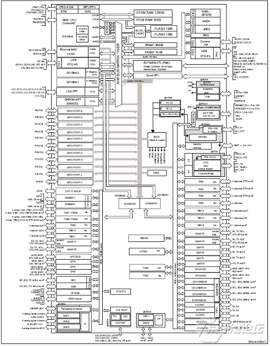
图1{京电港论坛}.STM32F777xx, STM32F778Ax和STM32F779xx框架图
STM32F779NI MCU评估板STM32F779I-EVAL
The STM32F779I-EVAL evaluation board is a complete demonstration and development platform for STMicroelectronics ARM® Cortex®-M7 core-based STM32F779NI microcontrollers. It features the following interfaces: four I2Cs, six SPIs with three multiplexed full-duplex I2S, SDIO, two SAIs, 8-bit to 14-bit digital camera, Ethernet MAC, FMC, Quad-SPI. It also features four USARTs and four UART peripherals, two CAN buses, three 12-bit ADC converters, two 12-bit DAC channels, internal 512 Kbytes of SRAM + 16 Kbytes of instruction, 2 Mbytes of Flash memory, TCM RAM + 4 Kbytes of backup SRAM, USB OTG HS and USB OTG FS peripherals, SWD and JTAG debugging support, Cryptographic acceleration (hardware acceleration for AES 128, 192, 256, triple DES, HASH (MD5, SHA-1, SHA-2), and HMAC). This evaluation board can be used as a reference design for user application development but it is not considered as a final application.
The full range of hardware features on the board helps the user to evaluate all the peripherals (USB OTG HS, USB OTG FS, Ethernet, motor control, microSD™ card, USART, audio DAC and ADC, digital microphone, CAN, SRAM, NOR Flash, SDRAM, Quad SPI Flash, 4" DSI LCD with capacitive touch panel etc.) and develop applications. Extension headers make provide an easy mean of connecting a daughterboard for a specific application.The integrated ST-LINK/V2-1 provides an embedded in-circuit debugger and programmer for the STM32.
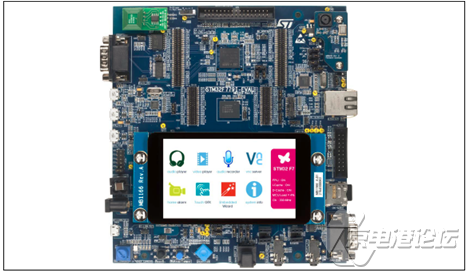
图2{京电港论坛}.评估板STM32F779I-EVAL外形实物图
评估板STM32F779I-EVAL主要特点:
• STM32F779I-EVALmicrocontroller with 2 Mbytes of Flash memory, internal 512 Kbytes of SRAM + 16 Kbytes of instruction and TCM RAM + 4 Kbytes of backup SRAM in BGA216 package
• Six options for 5V power supply:
C Power jack
C ST-LINK/V2-1 Micro-B USB connector
C User USB HS connector
C User USB FS1 connector
C User USB FS2 connector
C Daughterboard
• SAI interface audio codec, stereo audio jack which supports headset with microphone
• Two stereo digital microphones, audio jack connector used to connect external speakers
• 4-Gbyte (or more) SDIO interface microSD™ card
• I2C Extension interface
• RS-232 connector
• JTAG/SWD and ETM trace debug support, ST-LINK/V2-1 embedded
• IEEE-802.3-2002 compliant Ethernet connector
• Camera module
• 8Mx32bit SDRAM, 1Mx16bit SRAM and 8Mx16bit NOR Flash
• 512-Mbit Quad-SPI NOR Flash
• 4" capacitive touch LCD display with MIPI® DSI connector
• Joystick with 4-direction control and selector
• Reset, Wake Up/Tamper or key button
• 4-color user LEDs
• Extension and memory connectors for daughterboard or wrapping board
• USB OTG HS and FS with Micro-AB connectors
• RTC with backup battery
• CAN2.0A/B compliant connector
• Potentiometer
• Motor control connector
• Cryptographic acceleration
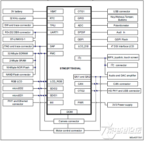
图3{京电港论坛}.评估板STM32F779I-EVAL硬件框架图
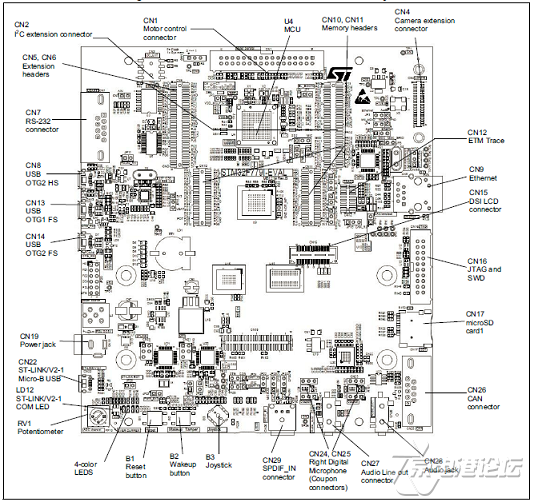
图4{京电港论坛}.评估板STM32F779I-EVAL元件结构图
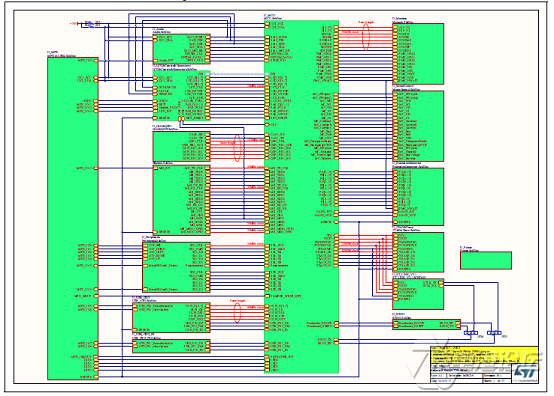
图5{京电港论坛}.评估板STM32F779I-EVAL电路原理图纸(1)
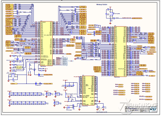
图6{京电港论坛}.评估板STM32F779I-EVAL电路原理图纸(2):MCU
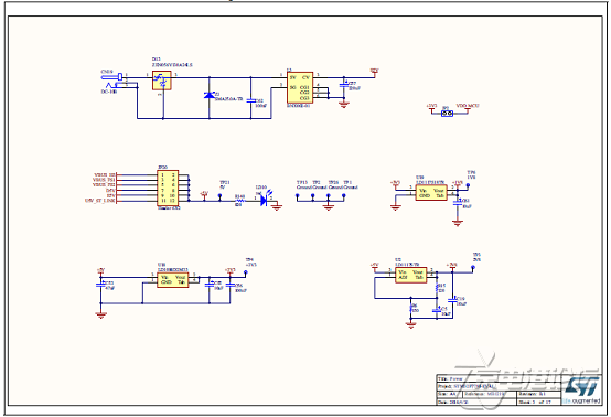
图7{京电港论坛}.评估板STM32F779I-EVAL电路原理图纸(3):电源
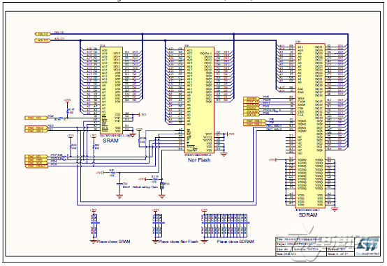
图8{京电港论坛}.评估板STM32F779I-EVAL电路原理图纸(4):SRAM,闪存,SDRAM
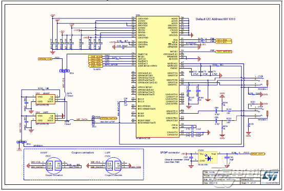
图9{京电港论坛}.评估板STM32F779I-EVAL电路原理图纸(5):音频
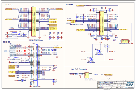
图1{京电港论坛}0.评估板STM32F779I-EVAL电路原理图纸(6):LCD,照相机,毗连器,
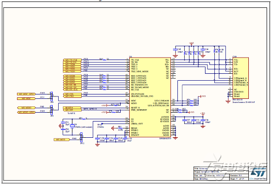
图1{京电港论坛}1.评估板STM32F779I-EVAL电路原理图纸(7):以太网
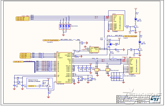
图1{京电港论坛}2.评估板STM32F779I-EVAL电路原理图纸(8):USB OTG HS
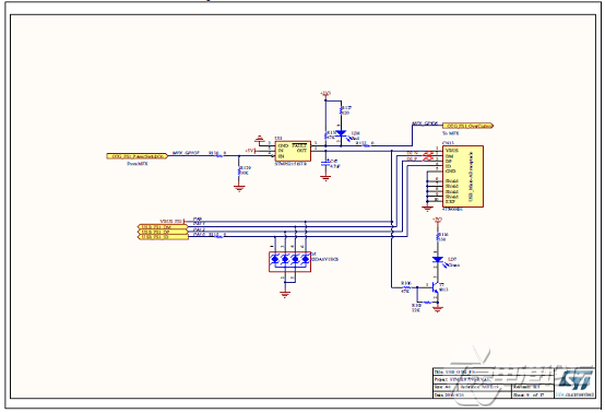
图1{京电港论坛}3.评估板STM32F779I-EVAL电路原理图纸(9):USB OTG FS
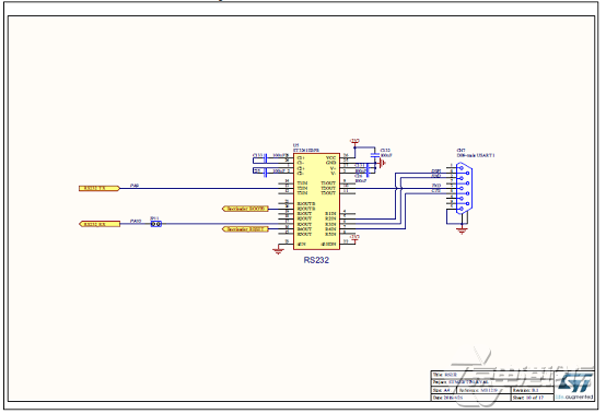
图1{京电港论坛}4.评估板STM32F779I-EVAL电路原理图纸(10):RS-232
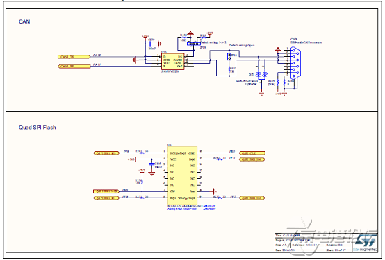
图1{京电港论坛}5.评估板STM32F779I-EVAL电路原理图纸(11):CAN,Quad-SPI
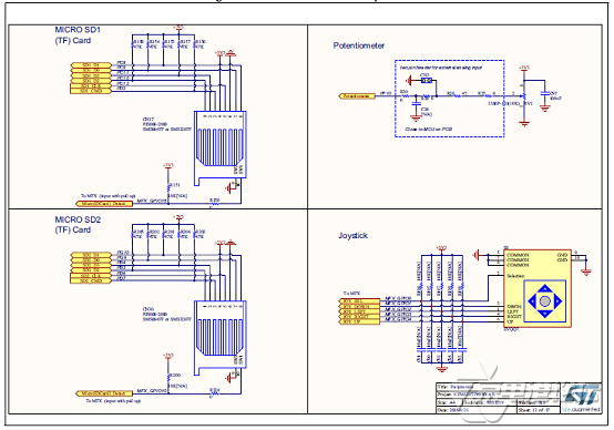
图1{京电港论坛}6.评估板STM32F779I-EVAL电路原理图纸(12):外设
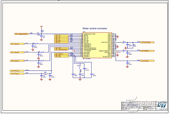
图1{京电港论坛}7.评估板STM32F779I-EVAL电路原理图纸(13):马达控制
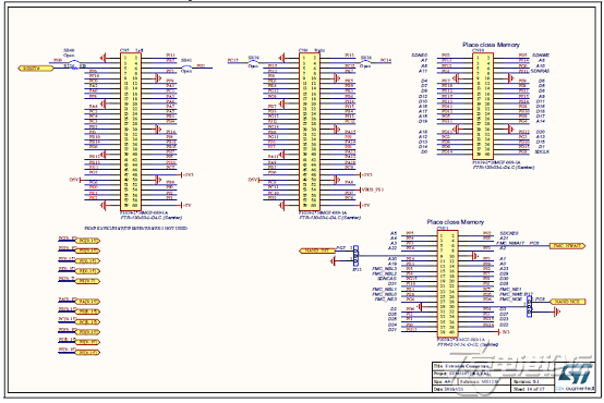
图1{京电港论坛}8.评估板STM32F779I-EVAL电路原理图纸(14):扩展毗连器
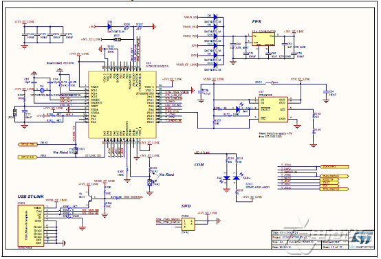
图1{京电港论坛}9.评估板STM32F779I-EVAL电路原理图纸(15):ST-LINKN2-1
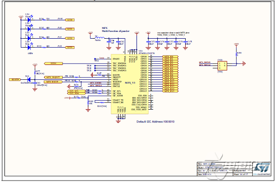
图2{京电港论坛}0.评估板STM32F779I-EVAL电路原理图纸(16):MFX和LED
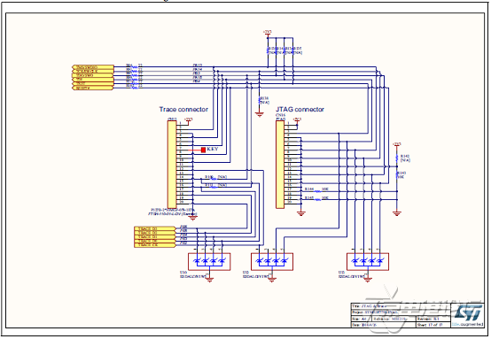
图2{京电港论坛}1.评估板STM32F779I-EVAL电路原理图纸(17):JTAG和跟踪
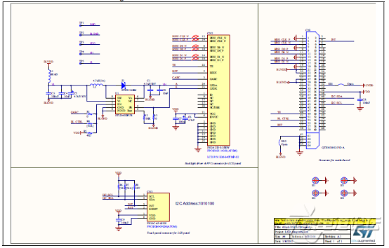
图2{京电港论坛}2.评估板STM32F779I-EVAL电路原理图纸(18):4DSI LCD板
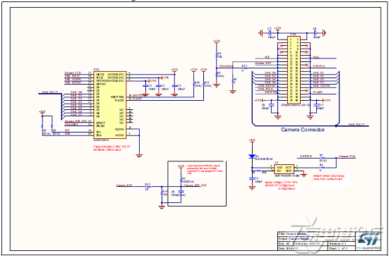
图2{京电港论坛}3.评估板STM32F779I-EVAL电路原理图纸(19):照相机模块
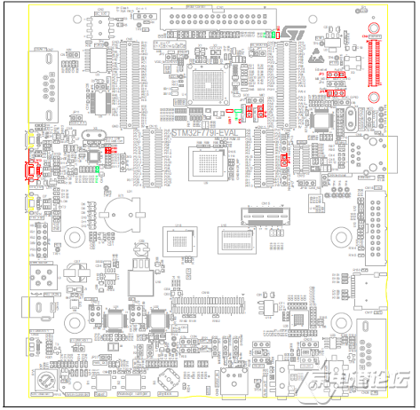
图2{京电港论坛}4.评估板STM32F779I-EVAL马达控制PCB线路板图(顶层)
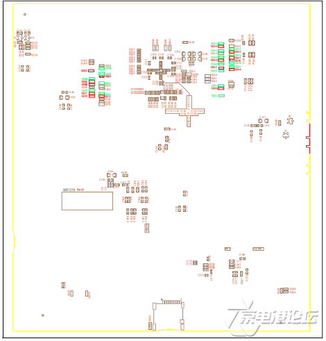
图2{京电港论坛}5.评估板STM32F779I-EVAL马达控制PCB线路板图(底层)
评估板STM32F779I-EVAL质料清单见:
 评估板STM32F779I-EVAL质料清单.zip
详情请复制打开此衔接地址:
http://www.st.com/content/ccc/resource/technical/document/datasheet/group3/8a/34
/ed/7e/4c/04/4b/7a/DM00225424/files/DM00225424.pdf/jcr:content/translations/en.DM00225424.pdf
和http://www.st.com/content/ccc/resource/technical/document/user_manual/group0/64/5f/b4/25/72
/a8/44/d9/DM00276570/files/DM00276570.pdf/jcr:content/translations/en.DM00276570.pdf
 en.DM00225424.pdf
en.DM00276570.pdf


 热点图文
热点图文