|
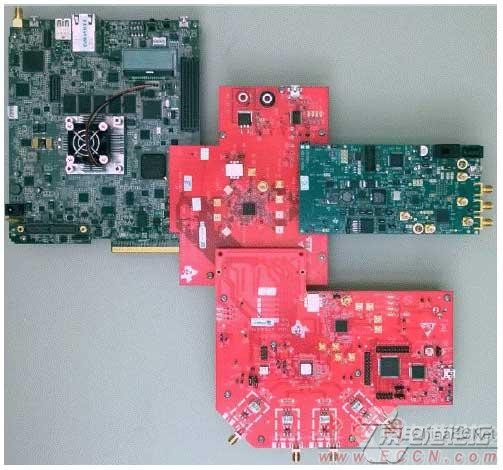
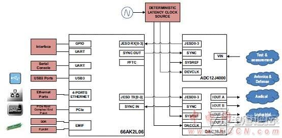
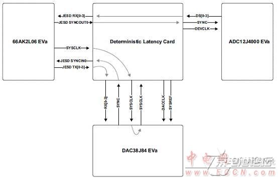
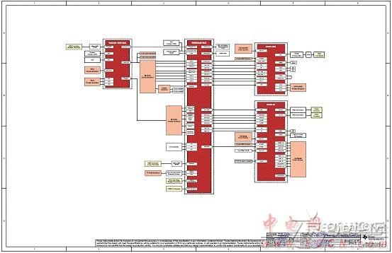
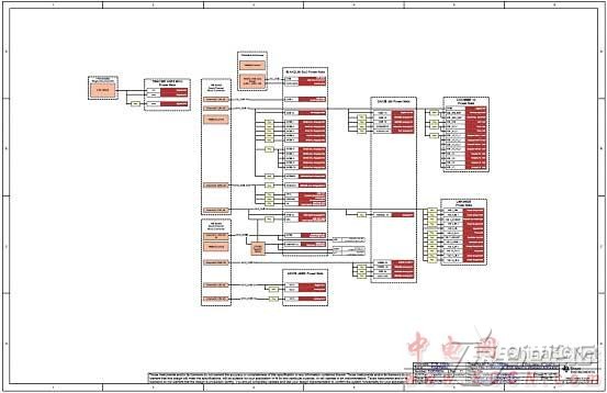
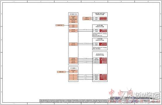
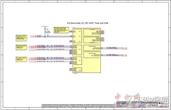
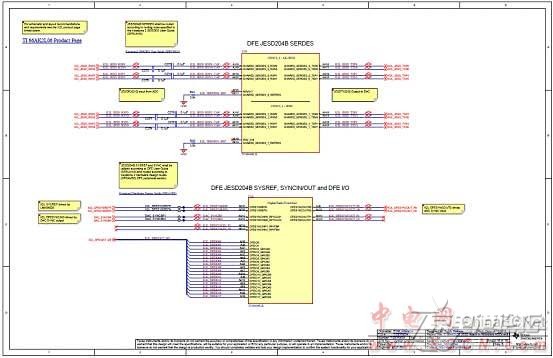
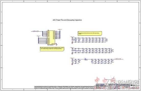
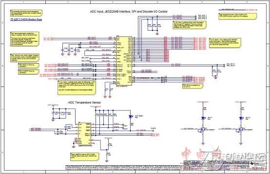
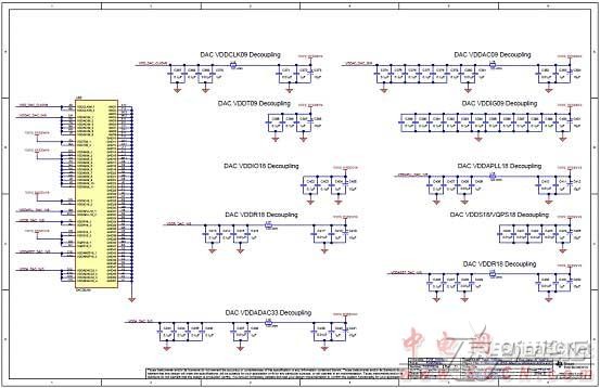
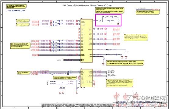
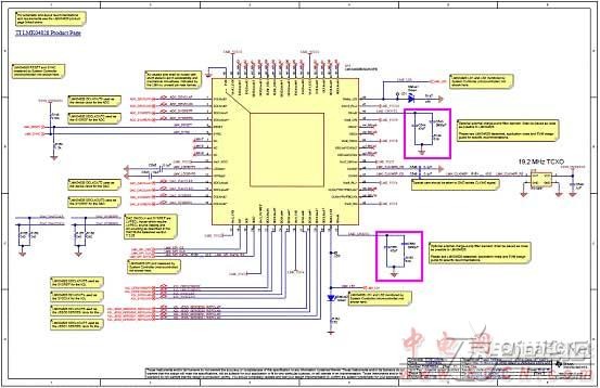
TI公司的66AK2L06 KeyStoneSoC是{方案}KeyStone II Multicore SoC架构的C66x系列产物,集成了多种子系统(ARM CorePac, C66x CorePacs, IP网络,数字前端,FFT处理),器件中的ARM和DSP核提供了极好的信号和控制处理性能,主要用在医疗电子,测试丈量,航空电子和军事以及工业控制.本京电港论坛文章先容了66AK2L06主要特点,框架图,以及66AK2L06 JESD Attach to ADC12J4000 / DAC38J84设计主要特性,系统框图,电路原理图纸和质料清单. The 66AK2L06 KeyStoneSoC is a member of the C66x family based on TI’s new KeyStone II Multicore SoC Architecture and is a low-power solution with integrated JESD204B lanes that meets the more stringent power, size, and cost requirements of applications requiring connectivity with ADC and DAC based applications. The device’s ARM and DSP cores deliver exceptional processing power on platforms requiring high signal and control processing. TI’s KeyStone II Architecture provides a programmable platform integrating various subsystems (ARM CorePac, C66x CorePacs, IP network, Digital Front End, and FFT processing) and uses a queue-based communication system that allows the SoC resources to operate efficiently and seamlessly. This unique SoC architecture also includes a TeraNet switch that enables the wide mix of system elements, from programmable cores to dedicated coprocessors and high-speed IO, to each operate at maximum efficiency with no blocking or stalling. The addition of the ARM CorePac in the 66AK2L06 device enables the ability for complex control code processing on-chip. Operations such as housekeeping and management processing can be performed with the Cortex-A15 processor. TI’s new C66x core launches a new era of DSP technology by combining fixed-point and floating-point computational capability in the processor without sacrificing speed, size, or power consumption. The raw computational performance is an industry-leading 38.4 GMACS/core and 19.2 Gflops/core (@ 1.2 GHz operating frequency). The C66x is also 100% backward compatible with software for C64x+ devices. The C66x CorePac incorporates 90 new instructions targeted for floating point (FPi) and vector math oriented (VPi) processing. The 66AK2L06 contains many coprocessors to offload the bulk of the processing demands of higher layers of application. This keeps the cores free for algorithms and other differentiating functions. The SoC contains multiple copies of key coprocessors such as the FFTC. The architectural elements of the SoC (Multicore Navigator) ensure that data is processed without any CPU intervention or overhead, allowing the system to make optimal use of its resources. TI’s scalable multicore SoC architecture solutions provide developers with a range of software-compatible and hardware-compatible devices to minimize development time and maximize reuse. The 66AK2L06 device has a complete set of development tools that includes: a C compiler, an assembly optimizer to simplify programming and scheduling, and a Windows and Linux debugger interface for visibility into source code execution. 66AK2L06主要特性: Four TMS320C66x DSP Core Subsystems (C66x CorePacs), Each With 66AK2L06 JESD Attach to ADC12J4000/DAC38J84设计 TI Designs provide the foundation that you need including methodology, testing and design files quickly evaluate and customize the system. TI Designs help you accelerate your time to market. The 66AK2L06 JESD Attach to ADC12J4000 / DAC38J84 Design Guide demonstrates performance of the high-speed JESD204B connectivity between the 66AK2L06 System-on-Chip (SoC) with industry-leading high-speed data convertors. This design also demonstrates the signal-processing power of 66AK2L06 hardware co-processors, DSP CorePacs, and control processing power using ARM® CorePacs. A highlevel hardware block diagram shown in Figure 3 explains high-level connectivity of the 66AK2L06 device with ADC12J4000 and DAC38J84 for different applications. Here, the analog input comes from an ADC that best matches the requirements of each industry application. The analog input will be sampled, digitized, and sent to the 66AK2L06 device over a JESD interface. The 66AK2L06 processes the received data using its internal hardware co-processors and sends the data out via any of the available interfaces including JESD, Ethernet, or PCIe. The JESD output from the 66AK2L06 can be sent over the JESD interface to DAC38J84 for converting digitized data to analog output. The 66AK2L06 JESD Attach to ADC12J4000 / DAC38J84 Design is well suited for applications such as: • Communications test: Mobile handset testers, radio communication analyzer, base station analyzer, RF test cards 66AK2L06 JESD Attach to ADC12J4000 / DAC38J84设计特性: • Easy Integration Of Signal Processor To Data Converters Over JESD204B 特性应用: • Test And Measurement |


 热点图文
热点图文