PowerInt公司的InnoSwitch™3-CP系列在单片IC内集成了低级和次级控制器以及安全尺度的反馈,具有多种掩护如线途经压和欠压保护,输出过压和过流限制,超温关断等,大大简化了反激电源转换器的设计和制造.本文先容了InnoSwitch™3-CP系列产物亮点,框图,范例应用电路,以及45W USB PD电源参考设计DER-536主要特点和指标,电路图,质料清单和PCB设计图.
The InnoSwitch™3-CP family of ICs dramatically simplifies the designand manufacture of flyback power converters, particularly thoserequiring high efficiency and/or compact size. The InnoSwitch3-CPfamily incorporates primary and secondary controllers and safety-ratedfeedback into a single IC.
InnoSwitch3-CP family devices incorporate multiple protection featuresincluding line over and under-voltage protection, output over-voltageand over-current limiting, and over-temperature shutdown. Devices areavailable that support the common combinations of latching andauto-restart behaviors required by applications such as quick chargeand USB PD designs. The devices are available with and withoutcable-drop compensation.
InnoSwitch™3-CP系列产品亮点:
Highly Integrated, Compact Footprint
• Up to 94% efficiency across full load range
• Quasi-Resonant (QR) / CCM flyback controller, 650 V or 725 V MOSFET4,secondary-side sensing and synchronous rectification driver
• Integrated FluxLink™, HIPOT-isolated, feedback link
• Easily interfaces to load-directed and fast charge protocol ICs
• Constant Power (CP) Profile minimizes charging time with continuousadjustment of output current and voltage
• Accurate CV/CC/CP, independent of external components
• External IS resistor allows custom CC programming
• Instantaneous transient response with 0%-100%-0% load step
EcoSmart™ C Energy Efficient
• Less than 15 mW no-load including line sense
• Easily meets all global energy efficiency regulations
• Low heat dissipation
Advanced Protection / Safety Features
• Secondary MOSFET or diode short-circuit protection
• Open SR FET-gate detection
• Fast input line UV/OV protection
Optional Features
• Cable-drop compensation with multiple settings
• Variable output voltage, constant current profiles
• Auto-restart or latching fault response for output OVP/UVP
• Multiple output UV fault thresholds
• Latching or hysteretic primary over-temperature protection
Full Safety and Regulatory Compliance
• Reinforced isolation
• Isolation voltage >4000 VAC
• 100% production HIPOT testing
• UL1577 and TUV (EN60950) safety approved
• Excellent noise immunity enables designs that achieve class “A”performance for EN61000-4; EN61000-4-2, 4-3 (30 V/m), 4-4, 4-5,4-6, 4-8 (100 A/m) and 4-9 (1000 A/m) and Ford FMC1278 (RI-115)
Green Package
• Halogen free and RoHS compliant
InnoSwitch™3-CP系列应用:
• High efficiency flyback designs up to 65 W
• USB PD / QC / proprietary protocol chargers
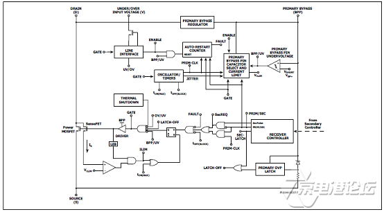
图1.InnoSwitch™3-CP系列初级控制器框图

图2.InnoSwitch™3-CP系列次级控制器框图
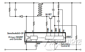
图3.InnoSwitch™3-CP系列典型应用电路图
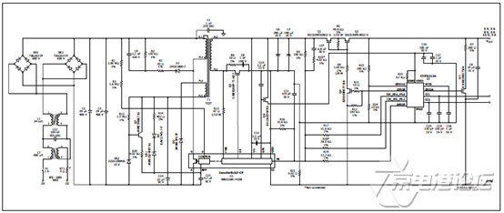
图4.InnoSwitch™3-CP系列应用电路:5V/3A,9V/3A,15V/3A USB PD 2.0兼容适配器
参考设计DER536
This document is an engineering report describing a 15 V / 3 A, 9 V / 3 A and 5 V / 3 A output USB Type-C and USB PD charger using the InnoSwitch3-CP INN3268C and Cypress CYPD2134 Type-C USB PD controller. This design shows the high power density and efficiency that is possible due to the high level of integration of the InnoSwitch3-CP controller providing exceptional performance.
This document contains the power supply specification, schematic, bill of materials, transformer documentation, printed circuit layout, safety and performance data
参考设计DER536主要特性:
InnoSwitch3-CP is the industry’s first AC/DC IC with isolated, safety rated integrated feedback
All the benefits of secondary-side control with the simplicity of primary-side regulation
Insensitive to transformer variation
Built in synchronous rectification for high efficiency
Meets DOE6 and CoC V5 2016 with at least 1.4% margin
<30 mW no-load input power across line
Load regulation ≤ 2.5%
Integrated thermal protection: passes thermals under ambient conditions of 45 ℃
Primary sensed overvoltage protection
Design thickness ≤10 mm without the enclosure
Planar transformer construction
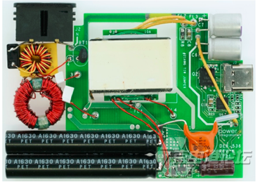
图5.参考设计DER536外形图(正面)
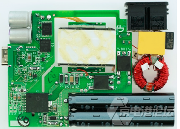
图6.参考设计DER536外形图(反面)
参考设计DER536主要性能指标:
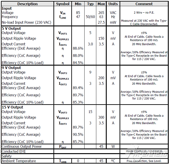
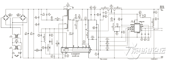
图7.参考设计DER536电路图
参考设计DER536材料清单:
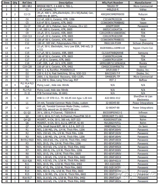


图8.参考设计DER536变压器电路图
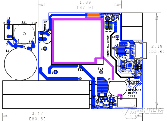
图9.参考设计DER536 PCB设计图(正面)
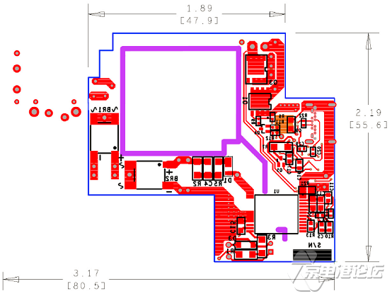
图10.参考设计DER536 PCB设计图(背面)
详情请见:

声明:京电港论坛转载作品均尽可能注明出处,该作品所有人的一切权利均不因本站而转移。
作者如不同意转载,既请通知本站予以删除或改正。转载的作品可能在标题或内容上或许有所改动。


 热点图文
热点图文