|
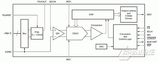
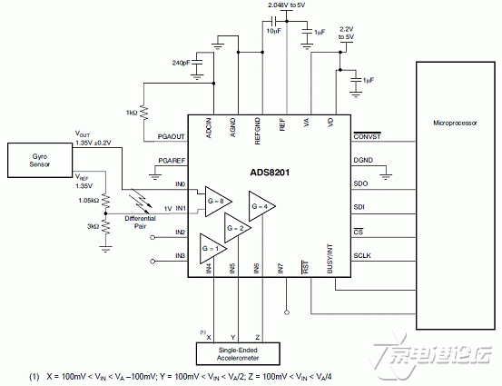
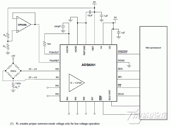
TI 公司的ADS8201是低功耗单片数据收罗系统,包罗12位接纳电容的SAR模数转换器(ADC),高性能一连时间可编增益放大器(PGA)以及全自动扫描8:1复接器,模拟电压2.2V到5.5V,高达100kSPS吞吐量速率, SCLK 高达25MHz (VD = 5V),主要用在手提通信,传感器接口,手提医疗仪表,数据收罗系统和GPS芯片组.本文先容ADS8201主要特点, 功能方框架图以及细密定位应用电路图和桥式传感器应用电路图. The ADS8201 is a low-power, complete on-chip data acquisition system optimized for portable applications that require direct connections, wide dynamic range, and automatic operation with very low power consumption. The device includes a 12-bit, capacitor-based, successive approximation register (SAR) analog-to-digital converter (ADC); a high-performance, continuous-time programmable gain amplifier (PGA); and a fully automatic scan, 8-to-1 multiplexer (mux) with breakout to allow for system design flexibility. Many other features are included to further optimize system operation. Conversion results may be saved in an onboard first-in/first-out (FIFO) buffer and read out at a later time. Each channel has a gain setting that can be loaded automatically when it is selected. ADS8201主要特点: • Multi-Chip Ready and Fully Enabled:234 • Low-Power, Flexible Supply Range: C 2.2V to 5.5V Analog Supply C 1.32mW (100kHz, +VA = 2.2V, +VD = 2.2V) C 4.5mW (100kHz, +VA = 5V, +VD = 5V) • Up to 100kSPS Throughput Rate • Excellent DC Performance: • Transducer Interfaces C ±0.5 LSB typ, ±1.5 LSB max INL • Portable Medical Instruments C ±0.5 LSB typ, ±1.0 LSB max DNL • Data Acquisition Systems C ±6 LSB Offset Error at +VA =5V • GPS Chipsets C ±0.1%FS Gain Error at +VA = 5V SPACE • Flexible Analog Inputs: C True Differential Input C Differential/Unipolar Input Range (0 to VREF) C TAG Bit Output C Programmable Averaging Function C Onboard, Eight Single-Ended/Four Differential Channel Mux: C High Input Impedance C High-Performance PGA (Gain = 1/2/4/8) C PGA Breakout C Auto/Manual Channel Select with Gain. C Auto/Manual Trigger C Mixed Type Partial Scan • Built-in Hardware Features: C On-chip Conversion Clock (CCLK) C Hardware/Software Reset C Programmable Status/Polarity for BUSY/INT • Flexible I/O: C SPI-/ DSP™-Compatible Serial Interface C Separate I/O Supply (2.2V to 5.5V) C Onboard 8×1 FIFO Buffer C SCLK up to 25MHz (VD = 5V) • Multi-Chip Ready and Fully Enabled: C Global CONVST (Independent of CS) • Power-Down Mode • 24-Pin 4×4 QFN Package ADS8201应用: • Portable Communications • Transducer Interfaces • Portable Medical Instruments • Data Acquisition Systems • GPS Chipsets 图3.ADS8201桥式传感器应用电路图 详情请复制打开此衔接地址: http://focus.ti.com/lit/ds/symlink/ads8201.pdf |


 热点图文
热点图文