MIcrosemi公司的SmartFusion2 SoC FPGA集成了第四代基于闪存的FPGA架构,一个ARM Cortex-M3处理器和高性能通信接口,具有业界最低功耗,最可靠和最安全的可编逻辑办理方案,主要应用在工业,国防,航空,通讯和医疗范畴.本文先容了SmartFusion2 SoC主要特点包罗可靠性,安全性, 低功耗, 高性能FPGA, 微控制器子系统, 时钟源, 高速串口, 高速存储器接口和工作电压和I/O等,框架图和芯片结构图以及SmartFusion2双轴马达控制板主要特点,框架图,电路图,质料清单和PCB设计原理图.
Microsemi SmartFusion®2 SoC FPGAs integrate the fourth generation flash-based FPGA fabric, an ARM Cortex-M3 processor, and high-performance communications interfaces on a single chip. The SmartFusion2 family is the industry’s lowest power, most reliable, and highest security programmable logic solution. SmartFusion2 FPGAs offer up to 3.6X the gate density, up to 2X the performance of previous flash-based FPGA families, and also include multiple memory blocks and multiply accumulate blocks for DSP processing. The 166 MHz ARM Cortex-M3 processor is enhanced with an embedded trace macrocell (ETM), memory protection unit (MPU), 8 Kbyte instruction cache, and additional peripherals, including controller area network (CAN), Gigabit Ethernet, and high-speed universal serial bus (USB). High-speed serial interfaces include PCI Express (PCIe), 10 Gbps attachment unit interface (XAUI) / XGMII extended sublayer (XGXS) plus native serialization/deserialization (SerDes) communication, while DDR2/DDR3 memory controllers provide high-speed memory interfaces.
SmartFusion2 SoC主要特点:
可靠性:
• Single event upset (SEU) immune
• Zero FIT FPGA configuration cells
• Junction temperature
• 125 °C―military temperature
• 100 °C―industrial temperature
• 85 °C―commercial temperature
• 125 °C―automotive
• Single error correct double error detect (SECDED) protection on the following:
• Ethernet buffers
• CAN message buffers
• Cortex-M3 embedded scratch pad memory (eSRAMs)
• USB buffers
• PCIe buffer
• DDR memory controllers with optional SECDED modes
• Buffers implemented with SEU resistant latches on the following:
• DDR bridges (MSS, MDDR, and FDDR)
• Instruction cache
• MMUART FIFOs
• SPI FIFOs
• NVM integrity check at power-up and on-demand
• No external configuration memory required―instant-on, retains configuration when powered off
安全性:
• Design security features (available on all devices)
• Intellectual property (IP) protection through unique security features and use models new to the PLD industry
• Encrypted user key and bitstream loading, enabling programming in less-trusted locations
• Supply-chain assurance device certificate
• Enhanced anti-tamper features
• Zeroization
• Data security features
• Non-deterministic random bit generator (NRBG)
• User cryptographic services (AES-256, SHA-256, and elliptical curve cryptographic (ECC) engine)
• User physically unclonable function (PUF) key enrollment and regeneration
• CRI pass-through DPA patent portfolio license
• Hardware firewalls protecting microcontroller subsystem (MSS) memories
低功耗:
• Low static and dynamic power
• Flash*Freeze (F*F) mode for fabric
• Power as low as 13 mW/Gbps per lane for SerDes devices
• Up to 50% lower total power than competing SoC devices
高性能FPGA:
• Efficient 4-input look-up tables (LUTs) with carry chains for high-performance and low power
• Up to 236 blocks of dual-port 18 Kbit SRAM (Large SRAM) with 400 MHz synchronous performance (512 x 36, 512 x 32, 1 kbit x 18, 1 kbit x 16, 2 kbit x 9, 2 kbit x 8, 4 kbit x 4, 8 kbit x 2, or 16 kbit x 1)
• Up to 240 blocks of three-port 1 Kbit SRAM with 2 read ports and 1 write port (micro SRAM)
• High-performance DSP signal processing
• Up to 240 fast mathblocks with 18 x 18 signed multiplication, 17 x 17 unsigned multiplication and 44-bit accumulator
微控制器子系统:
• Hard 166 MHz 32-Bit ARM Cortex-M3 processor
• 1.25 DMIPS/MHz
• 8 Kbyte instruction cache
• Embedded trace macrocell (ETM)
• Memory protection unit (MPU)
• Single cycle multiplication, hardware divide
• JTAG debug (4 wires), serial wire debug (SWD, 2 wires), and serial wire viewer (SWV)
interfaces
• 64 KB embedded SRAM (eSRAM)
• Up to 512 KB embedded nonvolatile memory (eNVM)
• Triple speed Ethernet (TSE) 10/100/1000 Mbps MAC
• USB 2.0 high speed on-the-go (OTG) controller with ULPI interface
• CAN controller, 2.0B compliant, conforms to ISO11898-1, 32 transmit and 32 receive buffers
• Two each: SPI, I2C, and multi-mode UARTs (MMUART) peripherals
• Hardware based watchdog timer
• One general purpose 64-bit (or two 32-bit) timer(s)
• Real-time calendar/counter (RTC)
• DDR bridge (4 port data R/W buffering bridge to DDR memory) with 64-bit AXI interface
• Non-blocking, multi-layer AHB bus matrix allowing multi-master scheme supporting 10 masters and 7 slaves
• Two AHB-Lite/APB3 interfaces to FPGA fabric (master/slave capable)
• Two DMA controllers to offload data transactions from the Cortex-M3 processor
• 8-channel peripheral DMA (PDMA) for data transfer between MSS peripherals and memory
• High-performance DMA (HPDMA) for data transfer between eSRAM and DDR memories
时钟源:
• Clock sources
• Up to two high precision 32 KHz to 20 MHz main crystal oscillator
• 1 MHz embedded RC oscillator
• 50 MHz embedded RC oscillator
• Up to 8 clock conditioning circuits (CCCs) with up to 8 integrated analog PLLs
• Output clock with 8 output phases and 45° phase difference (multiply/divide, and delay
capabilities)
• Frequency: input 1 MHz to 200 MHz, output 20 MHz to 400 MHz
高速串口:
• Up to 16 SerDes lanes, each supporting
• XGXS/XAUI extension (to implement a 10 Gbps (XGMII) Ethernet PHY interface)
• Native EPCS SerDes interface facilitates implementation of serial rapidIO (SRIO) in fabric or an SGMII interface to the Ethernet MAC in MSS
• PCI express (PCIe) endpoint controller
• ×1, ×2, and ×4 lane PCI express core
• Up to 2 Kbytes maximum payload size
• 64-Bit/32-Bit AXI and 64-Bit/32-Bit AHB master and slave interfaces to the application layer
高速存储器接口:
• Up to 2 high-speed DDRx memory controllers
• MSS DDR (MDDR) and fabric DDR (FDDR) controllers
• Supports LPDDR/DDR2/DDR3
• Maximum 333 MHz DDR clock rate
• SECDED enable/disable feature
• Supports various DRAM bus width modes, ×8, ×9, ×16, ×18, ×32, ×36
• Supports command reordering to optimize memory efficiency
• Supports data reordering, returning critical word first for each command
• SDRAM support through the SMC_FIC and additional soft SDRAM memory controller
工作电压和I/O:
• 1.2 V core voltage
• Multi-standard user I/Os (MSIO/MSIOD)
• LVTTL/LVCMOS 3.3 V (MSIO Only)
• LVCMOS 1.2 V, 1.5 V, 1.8 V, 2.5 V
• DDR (SSTL2_1, SSTL2_2)
• LVDS, MLVDS, Mini-LVDS, RSDS differential standards
• PCI
• LVPECL (receiver only)
• DDR I/Os (DDRIO)
• DDR2, DDR3, LPDDR, SSTL2, SSTL18, HSTL
• LVCMOS 1.2 V, 1.5 V, 1.8 V, 2.5 V
• Market leading number of user I/Os with 5G SerDes
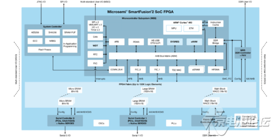
图1. SmartFusion2 SoC框架图
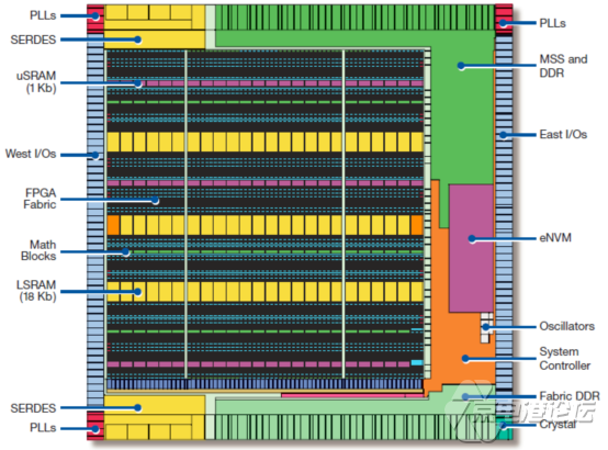
图2. SmartFusion2芯片结构图
SmartFusion2双轴马达控制板
The SmartFusion2 Dual-Axis Motor Control Starter Kit gives designers a starting point to evaluate time-saving and proven motor control reference designs. The kit is supplied with the hardware IP blocks and software. A fully integrated solution along with a powerful and easy to use GUI that enables designers to quickly prototype the design is also provided. The kit helps designers in customizing and developing dual-axis motor control solution on the SmartFusion2 device for a specific application and reduces time-to-market. This document provides details about the hardware setup and connections for running the demo design.
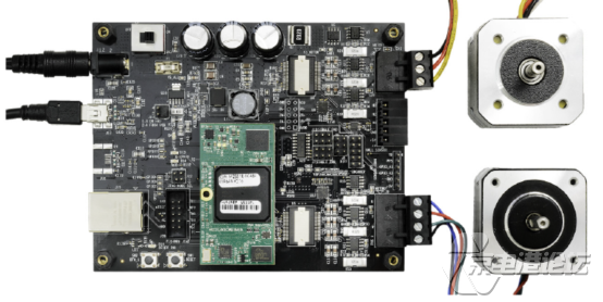
图3.SmartFusion2双轴马达控制板外形图
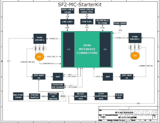
图4.SmartFusion2双轴马达控制板电路图(1)
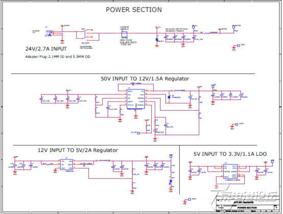
图5.SmartFusion2双轴马达控制板电路图(2)
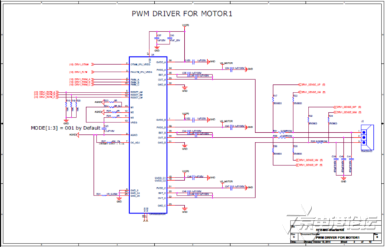
图6.SmartFusion2双轴马达控制板电路图(3)
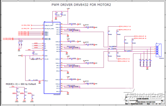
图7.SmartFusion2双轴马达控制板电路图(4)
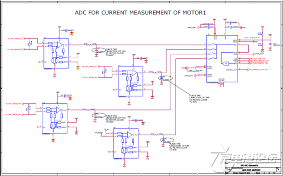
图8.SmartFusion2双轴马达控制板电路图(5)
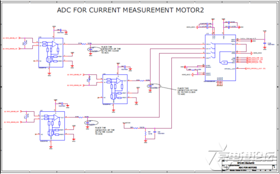
图9.SmartFusion2双轴马达控制板电路图(6)
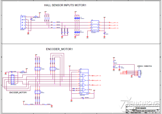
图10.SmartFusion2双轴马达控制板电路图(7)
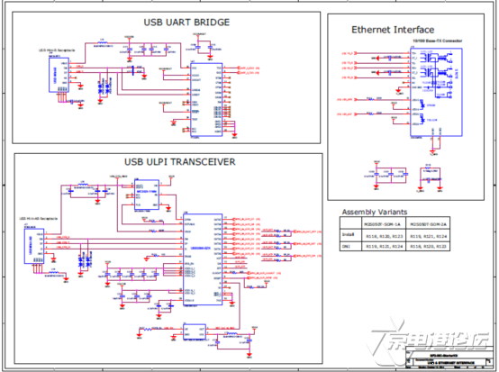
图11.SmartFusion2双轴马达控制板电路图(8)
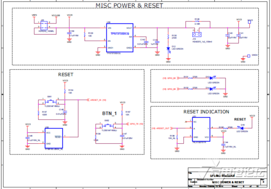
图12.SmartFusion2双轴马达控制板电路图(9)

图13.SmartFusion2双轴马达控制板电路图(10)
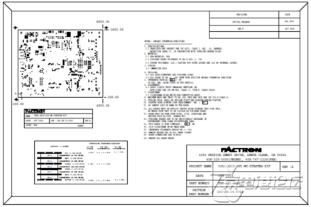
图14.SmartFusion2双轴马达控制板PCB设计原理图
SmartFusion2双轴马达控制板质料清单见:
详情请复制打开此衔接地址:
http://www.microsemi.com/products/fpga-soc/soc-fpga/smartfusion2#documentation
 Microsemi_SmartFusion2_Dual_Axis_Motor_Control_Starter_Kit_Demo_Guide(1).pdf
Microsemi_Smartfusion2_Product_Brief.pdf
 SmartFusion2双轴马达控制板质料清单.xls


 热点图文
热点图文