ST公司的STM32F756xx系列是基于高性能ARM®Cortex®-M7内核的32位RISC MCU,工作频率高达216MHz,具有单浮点单位(SFPU)精度,支持所有的ARM单精度数据处理指令和数据范例.集成了高达1MB闪存,320KB SRAM,16KB TCM RAM,4KB备份SRAM,满意高速或多通道音视频,无线通信,运动识别或电机控制的需求.本文先容了STM32F756xx系列主要特点,框架图,以及评估板STM32756G-EVAL主要特点,框架图,电路图和质料清单.
The STM32F756xx devices are based on the high-performance ARM®Cortex®-M7 32-bit RISC core operating at up to 216 MHz frequency. The Cortex®-M7 core features a single floating point unit (SFPU) precision which supports all ARM®single-precision data-processing instructions and data types. It also implements a full set of DSP instructions and a memory protection unit (MPU) which enhances the application security.
The STM32F756xx devices incorporate high-speed embedded memories with Flash memory up to 1 Mbyte, 320 Kbytes of SRAM (including 64 Kbytes of Data TCM RAM for critical real time data), 16 Kbytes of instruction TCM RAM (for critical real time routines), 4 Kbytes of backup SRAM available in the lowest power modes, and an extensive range of enhanced I/Os and peripherals connected to two APB buses, two AHB buses, a 32-bit multi-AHB bus matrix and a multi layer AXI interconnect supporting internal and external memories access.
All devices offer three 12-bit ADCs, two DACs, a low-power RTC, thirteen general-purpose 16-bit timers including two PWM timers for motor control and one low-power timer available in Stop mode, two general-purpose 32-bit timers, a true random number generator (RNG), and a cryptographic acceleration cell. They also feature standard and advanced communication interfaces.
STM32F756xx系列主要特点:
Core: ARM® 32-bit Cortex®-M7 CPU with FPU, adaptive real-time accelerator (ART Accelerator™) and L1-cache: 4KB data cache and 4KB instruction cache, allowing 0-wait state execution from embedded Flash memory and external memories, frequency up to 216 MHz, MPU, 462 DMIPS/2.14 DMIPS/MHz (Dhrystone 2.1), and DSP instructions.
Memories
Up to 1MB of Flash memory
1024 bytes of OTP memory
SRAM: 320KB (including 64KB of data TCM RAM for critical real time data) + 16KB of instruction TCM RAM (for critical real time routines) + 4KB of backup SRAM (available in the lowest power modes)
Flexible external memory controller with up to 32-bit data bus: SRAM, PSRAM, SDRAM/LPSDR SDRAM, NOR/NAND memories
Dual mode Quad-SPI
LCD parallel interface, 8080/6800 modes
LCD-TFT controller up to XGA resolution with dedicated Chrom-ART Accelerator™ for enhanced graphic content creation (DMA2D)
Clock, reset and supply management
1.7 V to 3.6 V application supply and I/Os
POR, PDR, PVD and BOR
Dedicated USB power
4-to-26 MHz crystal oscillator
Internal 16 MHz factory-trimmed RC (1% accuracy)
32 kHz oscillator for RTC with calibration
Internal 32 kHz RC with calibration
Low-power
Sleep, Stop and Standby modes
VBATsupply for RTC, 32×32 bit backup registers + 4KB backup SRAM
3×12-bit,2.4 MSPS ADC: up to 24 channels and 7.2 MSPS in triple interleaved mode
2×12-bit D/A converters
Up to 18 timers: up to thirteen 16-bit (1x low- power 16-bit timer available in Stop mode) and two 32-bit timers, each with up to 4 IC/OC/PWM or pulse counter and quadrature (incremental) encoder input. All 15 timers running up to 216 MHz. 2x watchdogs, SysTick timer
General-purpose DMA: 16-stream DMA controller with FIFOs and burst support
Debug mode
SWD & JTAG interfaces
Cortex®-M7 Trace Macrocell™
Up to 168 I/O ports with interrupt capability
Up to 164 fast I/Os up to 108 MHz
Up to 166 5 V-tolerant I/Os
Up to 25 communication interfaces
Up to 4× I2C interfaces (SMBus/PMBus)
Up to 4 USARTs/4 UARTs (27 Mbit/s, ISO7816 interface, LIN, IrDA, modem control)
Up to 6 SPIs (up to 50 Mbits/s),3 with muxed simplex I2S for audio class accuracy via internal audio PLL or external clock
2 x SAIs (serial audio interface)
2 × CANs (2.0B active) and SDMMC interface
SPDIFRX interface
HDMI-CEC
Advanced connectivity
USB 2.0 full-speed device/host/OTG controller with on-chip PHY
USB 2.0 high-speed/full-speed device/host/OTG controller with dedicated DMA, on-chip full-speed PHY and ULPI
10/100 Ethernet MAC with dedicated DMA: supports IEEE 1588v2 hardware,MII/RMII
8- to 14-bit parallel camera interface up to 54 Mbytes/s
Cryptographic acceleration: hardware acceleration for AES 128, 192, 256, triple DES, HASH (MD5, SHA-1, SHA-2), and HMAC
True random number generator
CRC calculation unit
RTC: subsecond accuracy, hardware calendar
96-bit unique ID
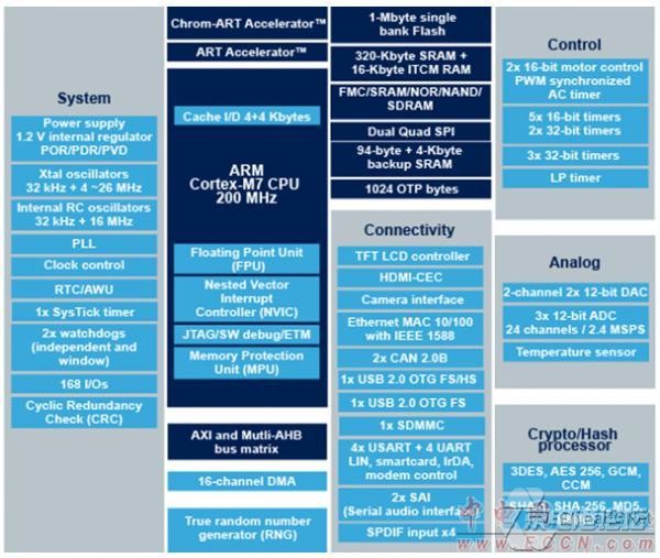
图1.STM32F756xx系列框架图
评估板STM32756G-EVAL
The STM32756G-EVAL evaluation board is a complete demonstration and development platform for STMicroelectronics ARM® Cortex®-M7 core-based STM32F756NGH6 microcontrollers. It features four I2C interfaces, six SPIs with three mutiplexed simplex I2S interfaces, SDMMC, four USARTs, two CANs, three 12-bit ADCs, two 12-bit DACs, two SAIs, 8- to 14-bit digital camera module interface, internal 320+4 Kbytes SRAM and 1 Mbytes Flash, USB HS OTG and USB FS OTG, Ethernet MAC, FMC interface, Quad-SPI interface, Cryptographic acceleration, JTAG debugging support. This evaluation board can be used as a reference design for user application development but it is not considered as a final application.
The full range of hardware features on the board helps the user to evaluate all peripherals (USB OTG HS, USB OTG FS, Ethernet, Motor Control, CAN, microSD Card, USART, Audio DAC and ADC, digital microphone, IrDA, RF-EEPROM, SRAM, Nor Flash, SDRAM, Quad-SPI Flash, 5.7" TFT LCD with capacitive touch panel and others) and develop his own applications. Extension headers make it possible to easily connect a daughterboard for a specific application. The integrated ST-LINK/V2-1 provides an embedded in-circuit debugger and programmer for the STM32 MCU.
评估板STM32756G-EVAL主要特点:
STM32F756NGH6 microcontroller with 1 Mbyte Flash and 320+4 Kbytes RAM
Six 5 V power supply options:
Power jack
ST-LINK/V2-1 USB connector
User USB HS connector
User USB FS1 connector
User USB FS2 connector
Daughterboard
SAI Audio DAC, stereo audio jack which supports headset with microphone
Stereo digital microphone, audio jack connector used to connect external speakers
2 Gbytes (or more) SDMMC interface microSD card
RF-EEPROM on I2C compatible serial interface
RS-232 communication
IrDA transceiver
JTAG/SWD and ETM trace debug support, ST-LINK/V2-1 embedded
IEEE-802.3-2002 compliant Ethernet connector
Camera module
8Mx32bit SDRAM, 1Mx16bit SRAM & 8Mx16bit Nor Flash
512MbitsQuadSPI Nor Flash
5.7 inch 640x480 pixel TFT color LCD with capacitive touch panel
Joystick with 4-direction control and selector.
Reset, WakeUp/Tamper or key button
4 color user LEDs
Extension connectors and memory connectors for daughterboard or wrapping board
USB OTG HS and FS with Micro-AB connectors
RTC with backup battery
CAN 2.0A/B compliant connection
Potentiometer
Motor control connector
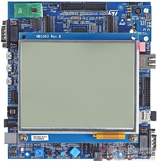
图2.评估板STM32756G-EVAL外形图
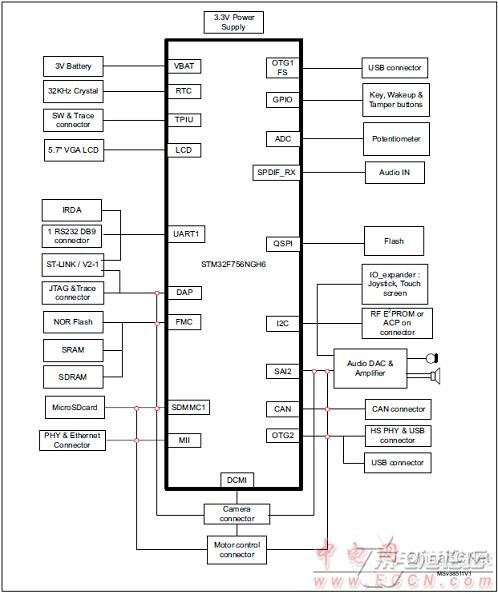
图3.评估板STM32756G-EVAL框架图
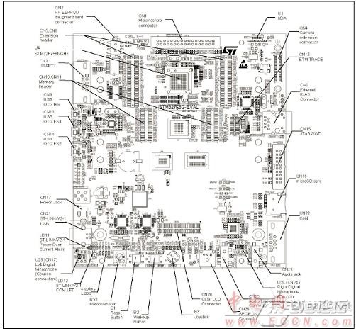
图4.评估板STM32756G-EVAL主要元件结构图
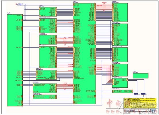
图5.评估板STM32756G-EVAL电路图

图6.评估板STM32756G-EVAL电路图:MCU
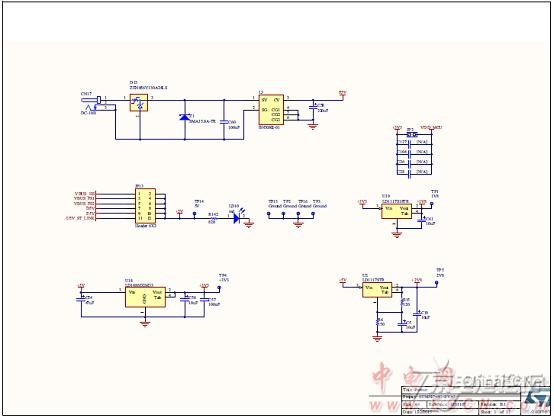
图7.评估板STM32756G-EVAL电路图:电源
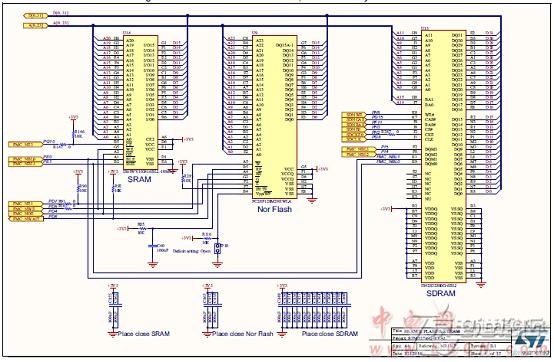
图8.评估板STM32756G-EVAL电路图:SRAM,闪存和DRAM
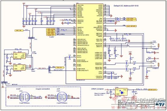
图9.评估板STM32756G-EVAL电路图:音频

图10.评估板STM32756G-EVAL电路图:LCD,照相机和RF毗连器
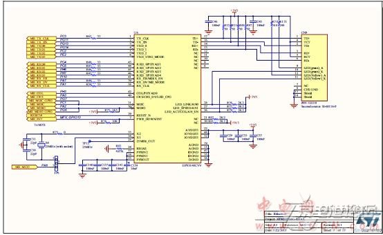
图11.评估板STM32756G-EVAL电路图:以太网
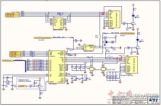
图12.评估板STM32756G-EVAL电路图:USB OTG HS和OTG FS2
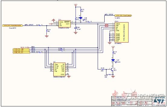
图13.评估板STM32756G-EVAL电路图:USB OTG FS1
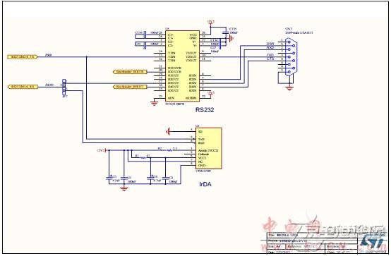
图14.评估板STM32756G-EVAL电路图:RS232和IrDA
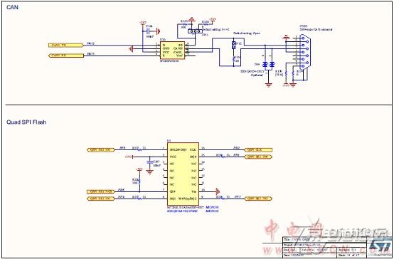
图15.评估板STM32756G-EVAL电路图:CAN和QSPI
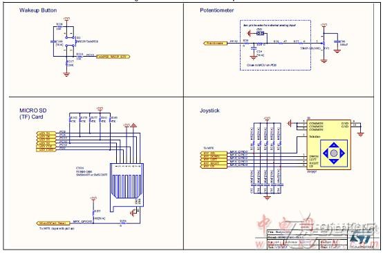
图16.评估板STM32756G-EVAL电路图:外设
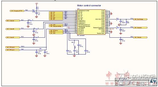
图17.评估板STM32756G-EVAL电路图:马达控制
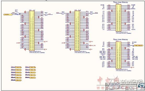
图18.评估板STM32756G-EVAL电路图:扩展毗连器
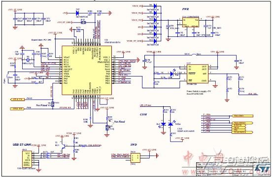
图19.评估板STM32756G-EVAL电路图:ST-LINK/V2-1

图20.评估板STM32756G-EVAL电路图:MFX
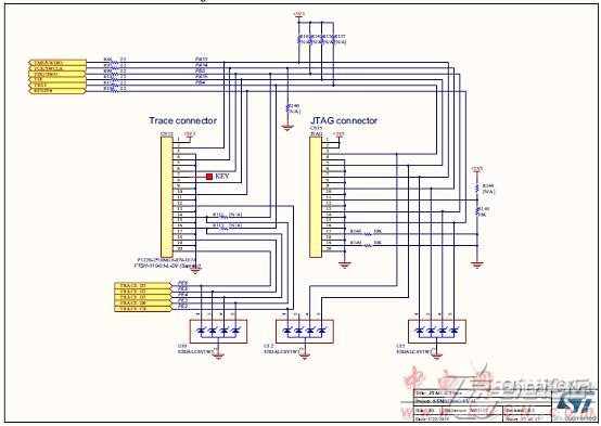
图21.评估板STM32756G-EVAL电路图:JTAG和Trace
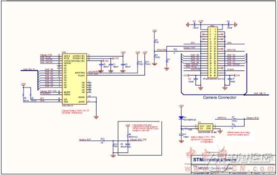
图22.评估板STM32756G-EVAL电路图:照相机子板
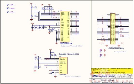
图23.评估板STM32756G-EVAL电路图:TFT LCD子板
评估板STM32756G-EVAL质料清单见:
 评估板STM32756G-EVAL质料清单.zip
详情请复制打开此衔接地址:
http://www.st.com/st-web-ui/static/active/en/resource/technical/document/datasheet/DM00166114.pdf
和http://www.st.com/st-web-ui/static/active/en/resource/technical/document/user_manual/DM00188617.pdf
 DM00166114.pdf
DM00188617.pdf
评估板STM32756G-EVAL电路文件.zip


 热点图文
热点图文