|
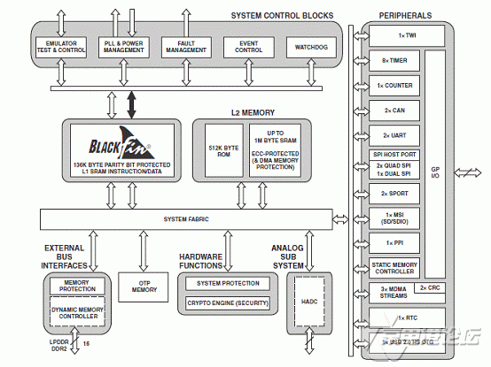
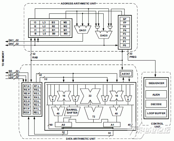
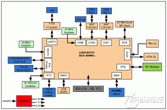
ADI公司的ADSP-BF70x Blackfin处理器系列接纳双MAC 16位最新的处理引擎,正交RISC类微处理器指令集,在单指令架构中接纳单指令多数据(SIMD)多媒体功能, Blackfin+核能工作高达400MHz,每周妻支持双16位或单32位MAC,其低功耗性能可应用在汽车电子,视频/图像分析,工业控制,马达控制,仪器仪表,电源控制和生物计量.本文先容了ADSP-BF70x Blackfin处理器系列主要特点,框架图和Blackfin+处理核框架图,以及评估板ADSP-BF707 EZ-KIT Lite 主要特点,框架图,电路图,质料清单和PCB结构设计原理图. The ADSP-BF70x processor is a member of the Blackfin family of products. The Blackfin processor combines a dual- MAC 16-bit state-of-the-art signal processing engine, the advantages of a clean, orthogonal RISC-like microprocessor instruction set, and single-instruction, multiple-data (SIMD) multimedia capabilities into a single instruction-set architecture. New enhancements to the Blackfin+ core add 32-bit MAC and 16-bit complex MAC support, cache enhancements, branch prediction and other instruction set improvements―all while maintaining instruction set compatibility to previous Blackfin products. The processor offers performance up to 400 MHz, as well as low static power consumption. Produced with a low-power and low-voltage design methodology, they provide world-class power management and performance. By integrating a rich set of industry-leading system peripherals and memory (shown in Table 1), the Blackfin processor is the platform of choice for next-generation applications that require RISC-like programmability, multimedia support, and leading-edge signal processing in one integrated package. These applications span a wide array of markets, from automotive systems to embedded industrial, instrumentation, video/image analysis, biometric and power/motor control applications. ADSP-BF70x Blackfin处理器系列主要特点: Blackfin+ core with up to 400 MHz performance BLACKFIN+ PROCESSOR CORE As shown in Figure 1, the processor integrates a Blackfin+ processor core. The core, shown in Figure 2, contains two 16-bit multipliers, one 32-bit multiplier, two 40-bit accumulators (which may be used together as a 72-bit accumulator), two 40- bit ALUs, one 72-bit ALU, four video ALUs, and a 40-bit shifter. The computation units process 8-, 16-, or 32-bit data from the register file. The compute register file contains eight 32-bit registers. When performing compute operations on 16-bit operand data, the register file operates as 16 independent 16-bit registers. All operands for compute operations come from the multiported register file and instruction constant fields. The core can perform two 16-bit by 16-bit multiply-accumu-lates or one 32-bit multiply-accumulate in each cycle. Signed and unsigned formats, rounding, saturation, and complex mul-tiplies are supported. The ALUs perform a traditional set of arithmetic and logical operations on 16-bit or 32-bit data. In addition, many special instructions are included to accelerate various signal processing tasks. These include bit operations such as field extract and pop-ulation count, divide primitives, saturation and rounding, and sign/exponent detection. The set of video instructions include byte alignment and packing operations, 16-bit and 8-bit adds with clipping, 8-bit average operations, and 8-bit subtract/absolute value/accumulate (SAA) operations. Also provided are the compare/select and vector search instructions. For certain instructions, two 16-bit ALU operations can be per-formed simultaneously on register pairs (a 16-bit high half and 16-bit low half of a compute register). If a second ALU is used, quad 16-bit operations are possible. The 40-bit shifter can perform shifts and rotates and is used to support normalization, field extract, and field deposit instructions 评估板ADSP-BF707 EZ-KIT Lite Thank you for purchasing the ADSP-BF707 EZ-KIT Lite®, Analog Devices, Inc. low-cost evaluation system for the ADSP-BF70x Blackfin® processors. The ADSP-BF707 processor is a member of the Blackfin family of products. Blackfin processors combine a dual-MAC state-of-the-art signal processing engine, the advantages of a clean, orthogonal RISC-like microprocessor instruction set, and single-instruction, multiple-data (SIMD)multimedia capabilities into a single instruction-set architecture. New enhancements to the Blackfin+™ core add 32-bit MAC and 16-bit complex MAC support, cache enhancements, branch prediction and other instruction set improvements―all while maintaining instruction set compatibility to previous Blackfin products. The EZ-KIT Lite is shipped with all of the necessary hardware―you can start the evaluation immediately. The package contains the standalone evaluation board, CE-approved power supply, and USB cable. The EZ-KIT Lite version ships with an ICE-1000 emulator, while the EZ-Board® version is supported by the ICE-1000 or ICE-2000 emulator.Expansion Interface III is provided for connecting a camera or audio extender board. Traditional mechanical switches for changing the board’s factory setup have been removed in favor of I2C controlled software switches. The only remaining mechanical switches are the boot mode switch and push buttons. The evaluation board is designed to be used in conjunction with the CrossCore® Embedded Studio (CCES) development tools to test capabilities of the ADSP-BF707 Blackfin processors. The CCES development environment aids advanced application code development and debug, such as: • Create, compile, assemble, and link application programs written in C++, C, and assembly 评估板ADSP-BF707 EZ-KIT Lite 主要特点: • Analog Devices ADSP-BF707 processor
更详细的评估板ADSP-BF707 EZ-KIT Lite PCB结构设计原理图见: 详情请复制打开此衔接地址:
|


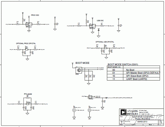
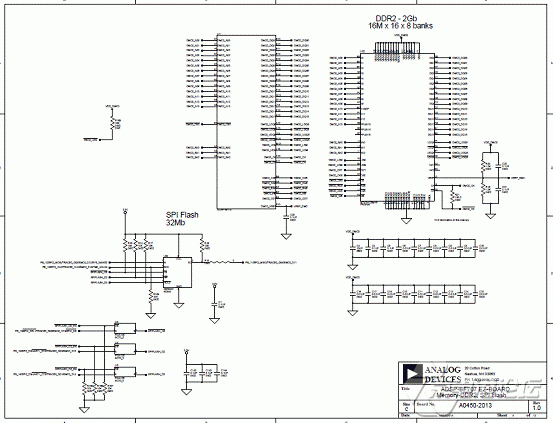
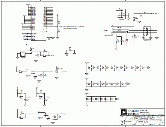


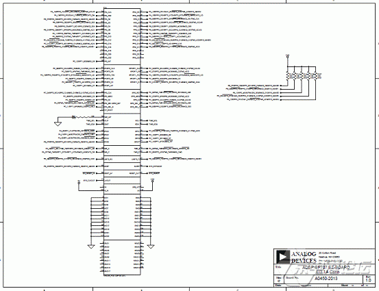


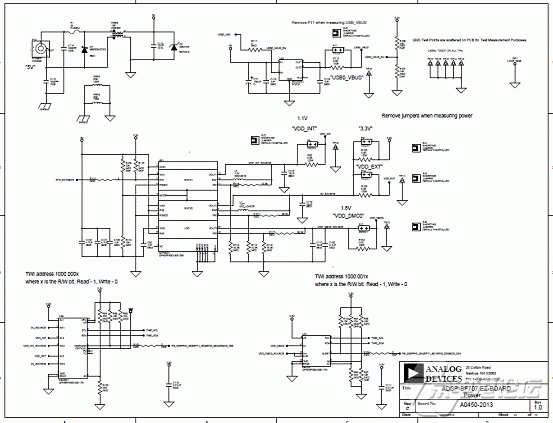


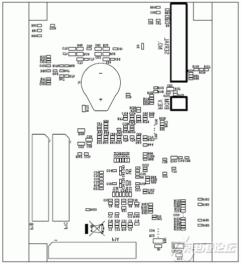
 评估板ADSP-BF707 EZ-KIT Lite PCB结构设计原理图.pdf


 热点图文
热点图文