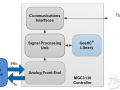
Maxim公司的MAX30110是完整的光学血氧和心率检测模拟前端(AFE),具有高分辨率光读出的信号处理通路,并内置了环境光消除和大电流LED驱动DAC,形成完整的光读出信号链.和蔼外接LED和光二极管,MAX30110是腕式应用的最低功耗最高性能心率检测解决方案.主电源1.8V,支持标准SPI兼容接口,主要用在腕式可穿戴设备,耳内可穿戴设备,SpO2监测设备和健身可穿戴设备.本文介绍了MAX30110主要优势和特性,框图,典型应用电路图以及评估板MAX30110 EVK包括Micro-PCB,传感器PCB1和传感器PCB2在内的主要特性,电路图,材料清单和详细的PCB设计图.
The MAX30110 is a complete optical pulse oximetry and heart rate detection integrated analog front-end. The MAX30110 has a high-resolution, optical readout signal-processing channel with built-in ambient light cancellation,as well as high-current LED driver DACs, to form a completeoptical readout signal chain. With external LED(s) and photo diode(s), the MAX30110 offers the lowest power, highest performance heart rate detection solution for wrist applications.
The MAX30110 operates on a 1.8V main supply voltage, with a separate 3.1V to 5.25V LED driver power supply. The device supports a standard SPI compatible interface, as well as shutdown modes through the software with near-zero standby current, allowing the power rails to remain powered at all times.
MAX30110主要优势和特性:
Reflective or Transmissive Heart Rate, Heart Rate Variability, or SpO2 Monitoring
Transmit SectionTwo 8-bit LED Current DACs
Four Current Ranges 50mA, 100mA, 150mA, 200mA
Low Noise Current Sources for High Peak Transmit to Receive Dynamic Range
Low 160mV Dropout to Support Direct Drive From Rechargeable Li Battery
High Output Impedance and High Supply Rejection to Support Unregulated Supply or Direct Drive From Boost Switcher Supply
Receive Section19-bit Optical ADC Path to Support the Lowest Perfusions Situations
Low 25pA-RMS Input Referred Noise to Minimize LED Power Under Most Conditions
High Ambient Light Input Range of 200μA and to Support Extraction of HRM Signal in the Most Adverse Lighting Conditions
Built-in Front And Back-End Ambient Light Cancellation,Improving Rejection and Eliminating SystemComplexity of Dealing with Ambient Light
Short Exposure Pulse Widths of 52μs, 104μs, 206μs, 417μs for Efficient Uses of LED Light
Multiple Sample Rate Options from 20sps to 3.2ksps
Ultra-Low-Power Operation for Mobile and Body-Wearable DeviceDynamic Power-Down Modes to 100sps forLow-Power Consumption
Full AFE Power Consumption of Less Than 25μA (Typ) at 25sps
Large 32 Sample FIFO to Support Batch Processing in the Microcontroller
Variety of System Monitors Mappable to Interrupts to Off-Load System Monitoring Functions From the Microcontroller
Low Shutdown Current = 1.4μA (typ)
SPI Interface
Supports a Single 1.8V Supply with Separate 3.1V to 5.25V LED Supply
Miniature 2.8mm x 2.0mm, 6x4, 0.4mm Ball Pitch WLP Package
-40 ℃ to +85℃ Operating Temperature Range
MAX30110应用:
Wrist-Worn Wearable Devices
In-Ear Wearable Devices
SpO2 Monitoring Devices
Fitness Wearable Devices
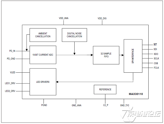
图1.MAX30110框图
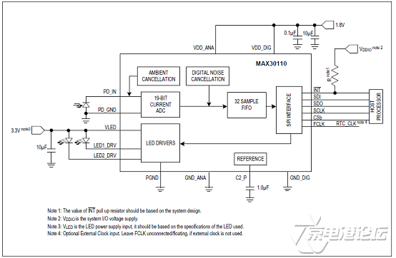
图2.MAX30110典型应用电路图
评估板MAX30110 EVK
The MAX30110 evaluation kit (EV kit) allows for the quick evaluation of the MAX30110 and MAX30112 optical AFE for applications at various sites on the body, particularly the wrist. MAX30110 supports standard SPI compatible interface, whereas MAX30112 supports I2C compatible interface. The EV kit allows flexible configurations to optimize measurement signal quality at minimal power consumption. The EV kit helps the user quickly learn how to configure and use the MAX30110 and MAX30112.
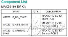
The EV kit consists of three boards. MAX30110_UC_ EVKIT is the main data acquisition board while MAX30110_ SFH7050_EVKIT and MAX30110_OSB_EVKIT are the sensor daughter boards in which the MAX30110 devices are placed in different optical configurations. The EV kit is powered using the USB supply to generate +1.8V for the AFE and accelerometer and +4.5V for the LEDs. The EV kit comes with a MAX30110EWG+ in a 24-bump wafer-level package (WLP).
评估板MAX30110 EVK主要特性:
Quick Evaluation of the MAX30110
Supports Optimization of Configurations
Facilitates Understanding MAX30110 Architecture and Solution Strategy
Real-Time Monitoring
Data-Logging Capabilities
USB-Powered
On-Board Accelerometer
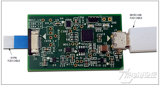
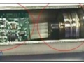
图3.评估板MAX30110 EVK硬件建立图(Micro-PCB)
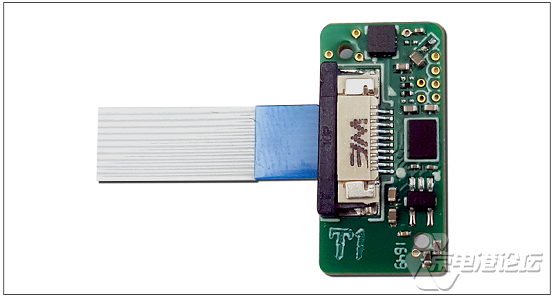
图4.评估板MAX30110 EVK硬件建立图(传感器PCB1)

图5.评估板MAX30110 EVK硬件建立图(传感器PCB1-顶视图)
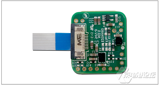
图6.评估板MAX30110 EVK硬件建立图(传感器PCB2-底视图)
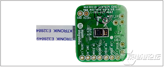
图7.评估板MAX30110 EVK硬件建立图(传感器PCB2-顶视图)
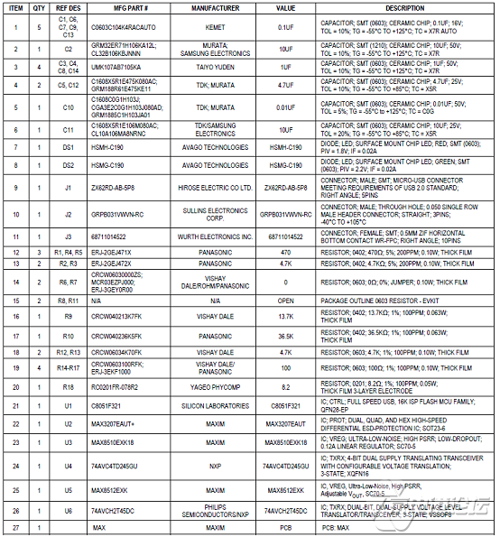
评估板MAX30110 EVK材料清单:
MAX30110_UC_EVKIT
MAX30110_OSB_EVKIT:

MAX30110_SFH7050_EVKIT:
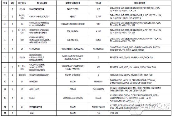

图8.MAX30110_UC_EVKIT电路图
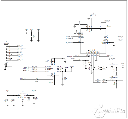
图9.MAX30110_OSB_EVKIT电路图

图10.MAX30110_SFH7050_EVKIT电路图

图11.MAX30110_UC_EVKIT PCB设计图:顶层丝印
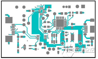
图12.MAX30110_UC_EVKIT PCB设计图:顶层
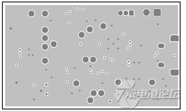
图13.MAX30110_UC_EVKIT PCB设计图:层2地GND
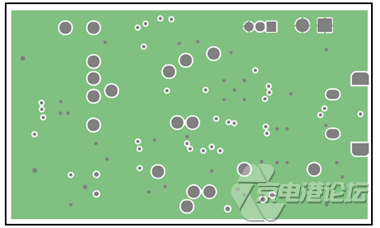
图14.MAX30110_UC_EVKIT PCB设计图:层3地GND

图15.MAX30110_UC_EVKIT PCB设计图:底层
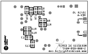
图16.MAX30110_UC_EVKIT PCB设计图:底层丝印
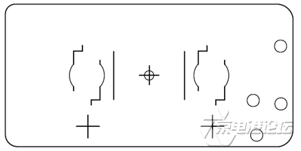
图17.MAX30110_OSB_EVKIT PCB设计图:顶层丝印
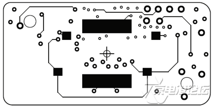
图18.MAX30110_OSB_EVKIT PCB设计图:顶层

图19.MAX30110_OSB_EVKIT PCB设计图:层2 SIGS

图20.MAX30110_OSB_EVKIT PCB设计图:层3GND

图21.MAX30110_OSB_EVKIT PCB设计图:层4 SIGS
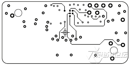
图22.MAX30110_OSB_EVKIT PCB设计图:层5 SIGS

图23.MAX30110_OSB_EVKIT PCB设计图:底层
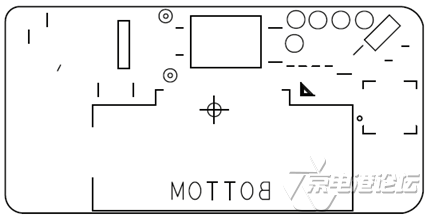
图24.MAX30110_OSB_EVKIT PCB设计图:底层丝印

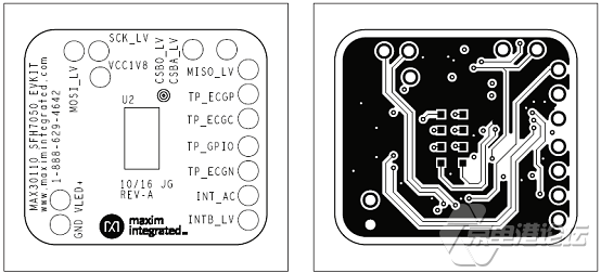
图25.MAX30110_SFH7050_EVKIT PCB设计图:左:顶层丝印;右:顶层

图26.MAX30110_SFH7050_EVKIT PCB设计图:电源

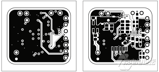
图27.MAX30110_SFH7050_EVKIT PCB设计图:左:GND;右:底层

图28.MAX30110_SFH7050_EVKIT PCB设计图:底层丝印
详情请见:


 热点图文
热点图文