Microsemi公司的RTG4是耐辐射系列FPGA,集成了Microsemi第四代{方案}闪存的FPGA架构和高性能接口如SERDES,LET的耐辐射大于110MeV.cm2/mg,高效4输入查找表(LUT)系统性能高达300MHz,多达209个双端口24.5位SRAM区块,同步性能300MHz,多达462个DSP算法区块(Mathblock),核电压1.2V,军用温度-55度C到125度C,主要用在空间飞行器(LEO, MEO, GEO, HEO,深度空间),高空飞行,医疗电子和核电厂控制.本京电港论坛文章先容了RTG4 FPGA特点和优势,框架图和RTG4 FPGA开辟板主要特点,主要元器件,框架图,电路原理图纸,质料清单和PCB线路板元件结构图.
RTG4™ FPGAs integrate Microsemi’s fourth-generation flash-based FPGA fabric and high-performanceinterfaces such as serialization/deserialization (SERDES) on a single-chip while maintaining theresistance to radiation-induced configuration upsets in the harshest radiation environments, such asspace flight (LEO, MEO, GEO, HEO, deep space), high altitude aviation, medical electronics, andnuclear power plant control. The RTG4 family offers up to 151,824 registers, which are hardened bydesign against radiation-induced single-event upsets (SEUs). Each RTG4 logic element includes a 4-input lookup table (LUT4) with fast carry chains providing high-performance FPGA fabric up to 300 MHz.
There are multiple embedded memory options and embedded multiply-accumulate blocks for digitalsignal processing (DSP) up to 300 MHz. A high-speed serial interface provides 3.125 Gbps nativeSERDES communication, while double data rate DDR2/DDR3/LPDDR memory controllers providehigh-speed memory interfaces..
RTG4 FPGAs integrate Microsemi’s fourth-generation flash-based FPGA fabric and high-performance interfaces such as serialization/deserialization (SERDES) on a single chip while maintaining the resistance to radiation-induced configuration upsets in the harshest radiation environments, such as space flight (LEO, MEO, GEO, HEO, deep space); high altitude aviation, medical electronics, and nuclear power plant control.
RTG4 FPGA特点和优势:
Radiation Tolerance
• Configuration Memory Upsets Immunity to LET > 110MeV.cm2/mg
• Single-Event Latch-up (SEL) Immunity to LET > 110MeV.cm2/mg
• SEU-Hardened Registers Eliminate the need forTriple-Module Redundancy (TMR)
C Immune to Single-Event Upsets (SEU) to LET > 37MeV.cm2/mg
C SEU Rate < 10-10 Errors/Bit-Day (GEO Solar Min)
• SRAM has built-in Error Detection and Correction (EDAC)
C Upset Rate < 10-10 Errors/Bit-Day (GEO Solar Min)
C Single-Bit Correction, Double-Bit Detection (SECDED)
• Single-event transient (SET) Upset Rate < 10-8 Errors/Bit-Day (GEO Solar Min) with Optional SET Filter
• Total Ionizing Dose (TID) > 100 Krad
High-Performance FPGA
• Efficient 4-Input Lookup Tables (LUTs) with Carry Chainsfor High System Performance up to 300 MHz without SETFilter
• Up to 209 blocks of Dual-Port 24.5 kbit SRAM (LargeSRAM) with 300 MHz Synchronous Performance (512 x 36,1 kbit x 18, 2 kbit x 9, 2 kbit x 12)
• Up to 462 DSP Mathblocks with 18-bit x 18-bit Input SignedMultiplication and 44-bit Output Accumulator
C High-Performance, 300 MHz (Without SET Filter) AcrossMilitary Temperature: -55C to 125C
• 16 SpaceWire Clock and Data Recovery Circuitry Instances,allowing High-Performance SpaceWire interface up to 400Mbit/sec.
High-Speed Serial Interfaces
24 Lanes of 3.125 Gbps Serialization/Deserialization(SERDES) supporting:
• XGXS/XAUI Extension (To implement a 10 Gbps XGMIIEthernet PHY interface)
• Native SERDES interface facilitates implementation ofSerial RapidIO in FPGA Fabric or an SGMII interface to aSoft Ethernet MAC
• PCI Express® (PCIe) Gen1 Hard IP Core
C x1, x2, x4 Lane(s) PCI Express Core
C Up to 2 Kbytes Maximum Payload Size
C 64-/32-bit AXI/AHB Master and Slave interfaces to theApplication Layer
High-Speed Memory Interfaces
Two High-Speed DDR2/DDR3 Memory Controllers:
• Supports DDR2 and DDR3 at 333 MHz (667 Mbps), LPDDRat 266 MHz (533 Mbps)-Max Clock Rate
• EDAC Option with SECDED
• Supports x9, x12, x18 and x36 Bus Widths
Specifications
• 1.2 V Nominal Core Voltage
• Single-Ended I/Os: LVCMOS 1.2 V to 3.3 V, LVTTL, PCI
• Voltage Reference I/Os with Performance at 600+ Mbps
C SSTL2, SSTL18, SSTL15, HSTL18, HSTL15
• True LVDS (600+ Mbps) Differential Receiver and True
Current-Mode Driver, with Built-in Termination
• Clock Sources Include High-Precision 50 MHz EmbeddedRC Oscillator
• Up to 8 Clock Conditioning Circuits (CCCs) with PLLs
C Frequency: Input 1 to 200 MHz, Output 20 to 400 MHz
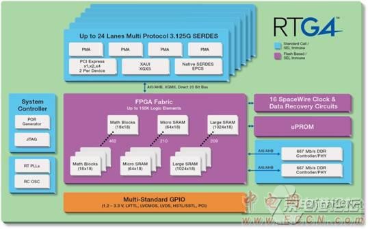
图1{京电港论坛}.RTG4 FPGA系列框架图
RTG4 FPGA开辟板
Microsemi’s RTG4™ Development Kit provides designers with an evaluation and development platform for applications such as: data transmission, serial connectivity, bus interface, and high-speed designs using the RTG4 devices. The development board features an RT4G150 device offering 151,824 logic elements in a ceramic package with 1,657 pins.
The RTG4 development board includes two 1GB Double Data Rate3 (DDR3) and 2Gb of SPI flash memories. The board also has several standard and advanced peripherals such as: PCIe x4 edge connector, two FMC connectors for using several off-the-shelf daughter cards, USB, Philips interintegrated circuit (I2C), gigabit Ethernet port, serial peripheral interface (SPI), and UART. A high precision operational amplifier circuitry on the board helps to measure the core power consumption by the device. There is a FlashPro programmer embedded on the board allowing programming of the RTG4 field programmable gate array (FPGA) through the JTAG interface.
The RTG4 Development Kit provides space customers with an evaluation and development platform for applications such as data transmission, serial connectivity, bus interface and high speed designs using RTG4 Radiation-Tolerant High-Density High-Performance FPGAs. The development board features a RT4G150 device offering more 150,000 logic elements in a Ceramic package with 1,657 pins.
RTG4 FPGA开辟板主要特点:
The RTG4-DEV-KIT device offers a full-featured 150,000 logic element (LE) RTG4 FPGA. This device has the following features integrated on a single chip:
• Radiation-Tolerant flash-based FPGA fabric.
• Industry standard 4-input lookup table-based (LUT) FPGA fabric with integrated math blocks.
• High-performance SERDES.
• Integrated hard DDR3 memory controllers with error correction.
• Static random-access memory (SRAM).
• Programmable read only memory (uPROM).
The RTG4 Development Kit has as the following standard interfaces:
• Two independent 1GB DDR3 synchronous dynamic random access memory (SDRAM).
• Two independent 1Gb SPI flash memories.
• PCIe (Gen1) x1 interface can be accessed through SMA cables.
• PCIe x4 edge connector.
• One pair SMA connectors for testing of the full-duplex SERDES channel.
• Two FMC connectors with HPC pinout for expansion.
• RJ45 interface for 10/100/1000 Ethernet.
• USB micro-AB connector.
• Headers for SPI, GPIOs.
• FTDI programmer interface to program the external SPI flash.
• JTAG programming interface.
• RVI header for application programming and debug.
• FlashPro4 or FlashPro5 programming header and embedded FlashPro5 programmer.
• Dual in-line package (DIP) switches for user application.
• Push-button switches and LEDs for demo purposes.
• Current measurement tes

图2{京电港论坛}.RTG4 FPGA开辟板框架图
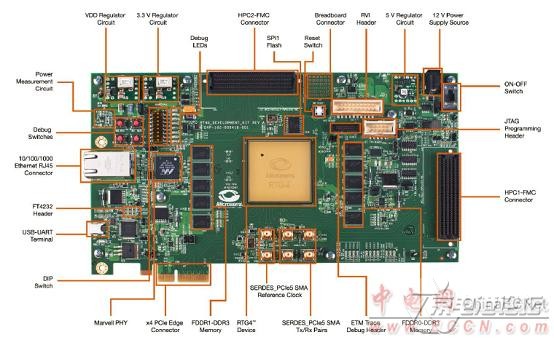
图3{京电港论坛}.RTG4 FPGA开辟板外形实物图
RTG4 FPGA开辟板硬件特点:
Two 1GB DDR3 synchronous dynamic random access memory (SDRAM)
2GB SPI flash memory
PCI Express Gen 1 x1 interface
PCIe x4 edge connector
One pair SMA connectors for testing of the full-duplex SERDES channel
Two FMC connectors with HPC/LPC pinout for expansion
RJ45 interface for 10/100/1000 Ethernet
USB micro-AB connector
Headers for SPI, GPIOs
FTDI programmer interface to program the external SPI flash
JTAG programming interface
RVI header for application programming and debug
Flashpro programming header
Embedded trace macro (ETM) cell header for debug
Dual in-line package (DIP) switches for user application
Push-button switches and LEDs for demo purposes
Current measurement test points
RTG4 FPGA开辟板包罗的元件:
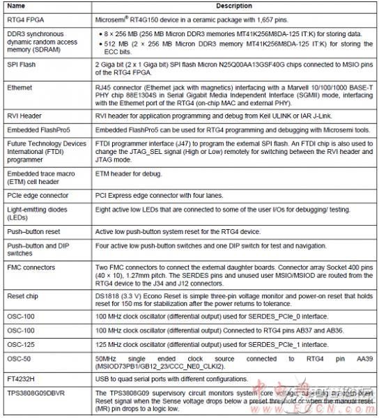


图4{京电港论坛}.RTG4 FPGA开辟板电路原理图纸(1)

图5{京电港论坛}.RTG4 FPGA开辟板电路原理图纸(2)

图6{京电港论坛}.RTG4 FPGA开辟板电路原理图纸(3)
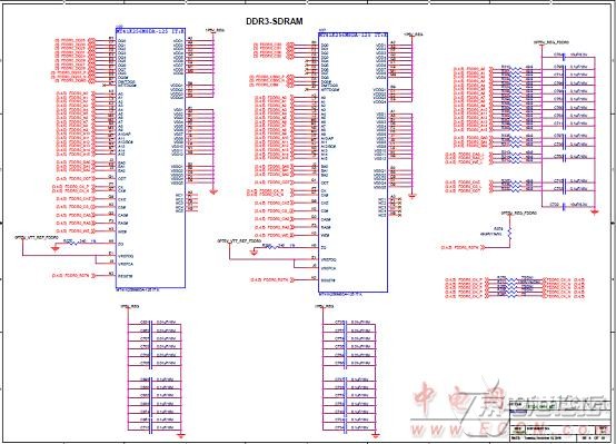
图7{京电港论坛}.RTG4 FPGA开辟板电路原理图纸(4)
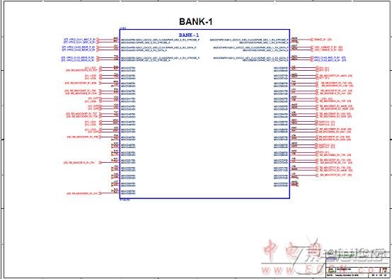
图8{京电港论坛}.RTG4 FPGA开辟板电路原理图纸(5)

图9{京电港论坛}.RTG4 FPGA开辟板电路原理图纸(6)
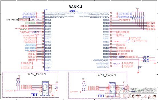
图1{京电港论坛}0.RTG4 FPGA开辟板电路原理图纸(7)
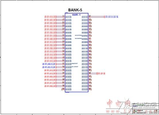
图1{京电港论坛}1.RTG4 FPGA开辟板电路原理图纸(8)

图1{京电港论坛}2.RTG4 FPGA开辟板电路原理图纸(9)

图1{京电港论坛}3.RTG4 FPGA开辟板电路原理图纸(10)
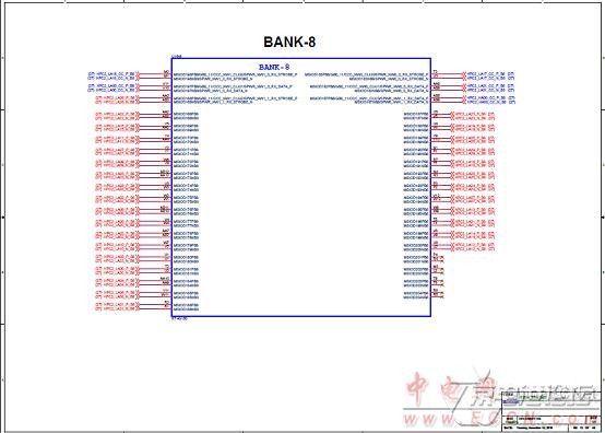
图1{京电港论坛}4.RTG4 FPGA开辟板电路原理图纸(11)
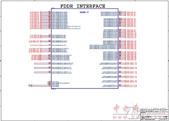
图1{京电港论坛}5.RTG4 FPGA开辟板电路原理图纸(12)
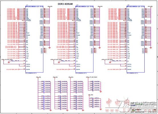
图1{京电港论坛}6.RTG4 FPGA开辟板电路原理图纸(13)
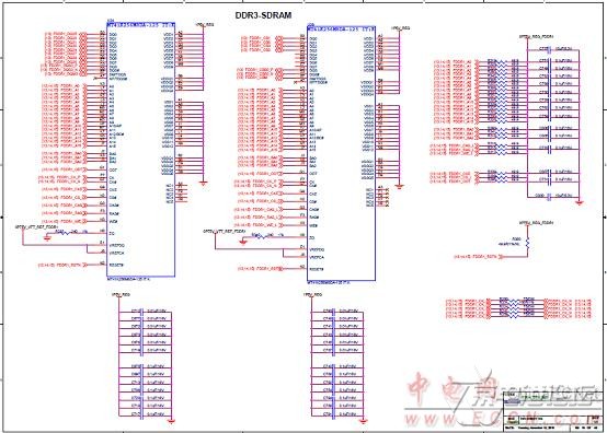
图1{京电港论坛}7.RTG4 FPGA开辟板电路原理图纸(14)

图1{京电港论坛}8.RTG4 FPGA开辟板电路原理图纸(15)

图1{京电港论坛}9.RTG4 FPGA开辟板电路原理图纸(16)

图2{京电港论坛}0.RTG4 FPGA开辟板电路原理图纸(17)
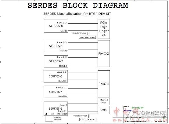
图2{京电港论坛}1.RTG4 FPGA开辟板电路原理图纸(18)

图2{京电港论坛}2.RTG4 FPGA开辟板电路原理图纸(19)
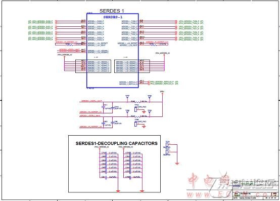
图2{京电港论坛}3.RTG4 FPGA开辟板电路原理图纸(20)
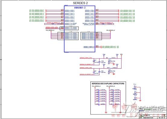
图2{京电港论坛}4.RTG4 FPGA开辟板电路原理图纸(21)
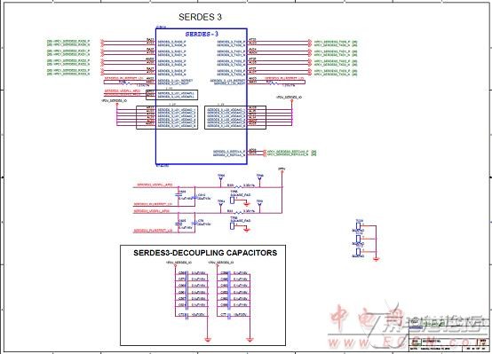
图2{京电港论坛}5.RTG4 FPGA开辟板电路原理图纸(22)
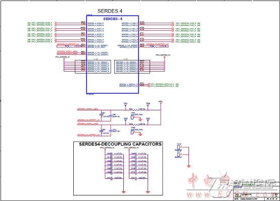
图2{京电港论坛}6.RTG4 FPGA开辟板电路原理图纸(23)
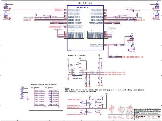
图2{京电港论坛}7.RTG4 FPGA开辟板电路原理图纸(24)

图2{京电港论坛}8.RTG4 FPGA开辟板电路原理图纸(25)
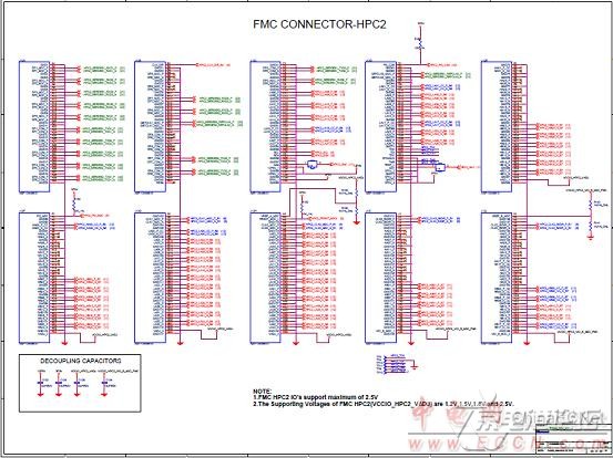
图2{京电港论坛}9.RTG4 FPGA开辟板电路原理图纸(26)

图3{京电港论坛}0.RTG4 FPGA开辟板电路原理图纸(27)
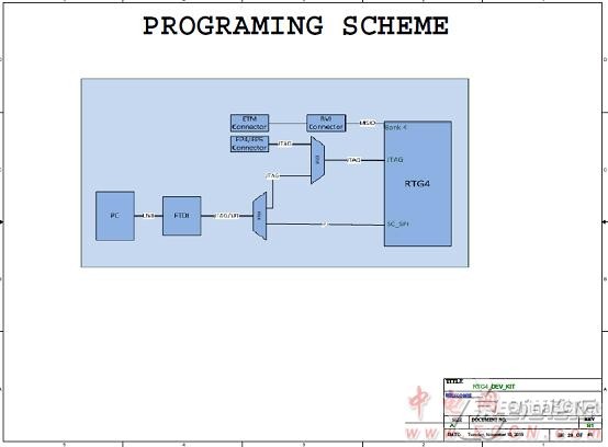
图3{京电港论坛}1.RTG4 FPGA开辟板电路原理图纸(28)
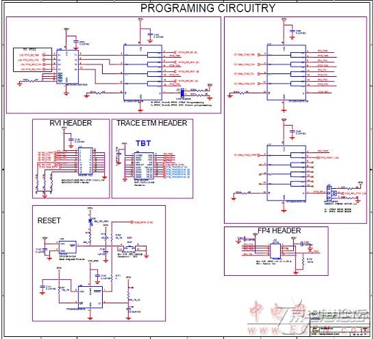
图3{京电港论坛}2.RTG4 FPGA开辟板电路原理图纸(29)

图3{京电港论坛}3.RTG4 FPGA开辟板电路原理图纸(30)

图3{京电港论坛}4.RTG4 FPGA开辟板电路原理图纸(31)

图3{京电港论坛}5.RTG4 FPGA开辟板电路原理图纸(32)
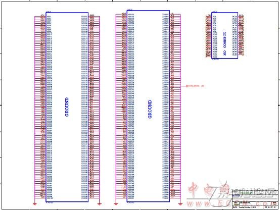
图3{京电港论坛}6.RTG4 FPGA开辟板电路原理图纸(33)
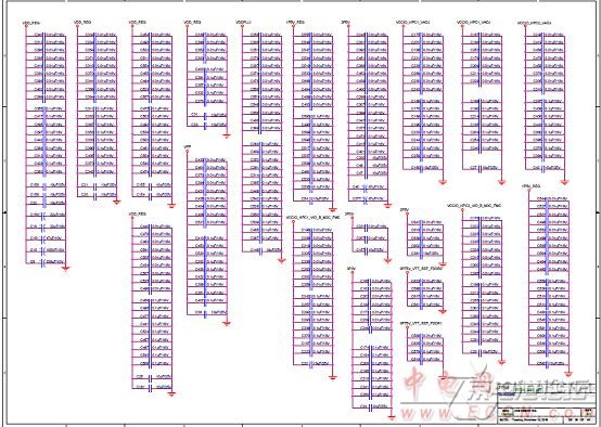
图3{京电港论坛}7.RTG4 FPGA开辟板电路原理图纸(34)
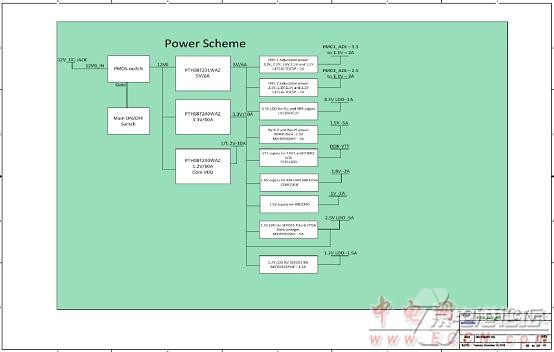
图3{京电港论坛}8.RTG4 FPGA开辟板电路原理图纸(35)
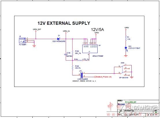
图3{京电港论坛}9.RTG4 FPGA开辟板电路原理图纸(36)
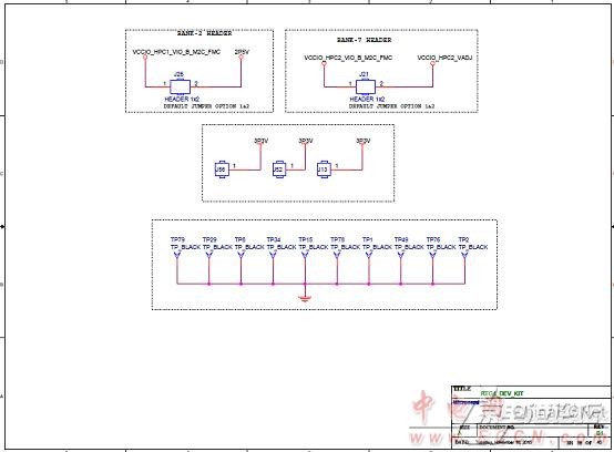
图4{京电港论坛}0.RTG4 FPGA开辟板电路原理图纸(37)
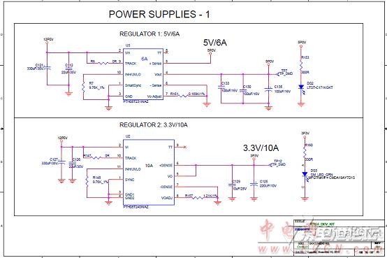
图4{京电港论坛}1.RTG4 FPGA开辟板电路原理图纸(38)

图4{京电港论坛}2.RTG4 FPGA开辟板电路原理图纸(39)
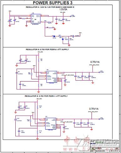
图4{京电港论坛}3.RTG4 FPGA开辟板电路原理图纸(40)
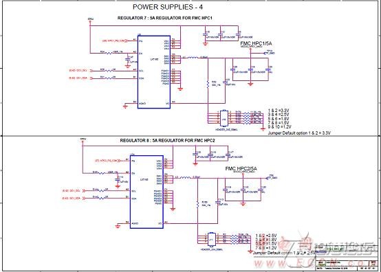
图4{京电港论坛}4.RTG4 FPGA开辟板电路原理图纸(41)
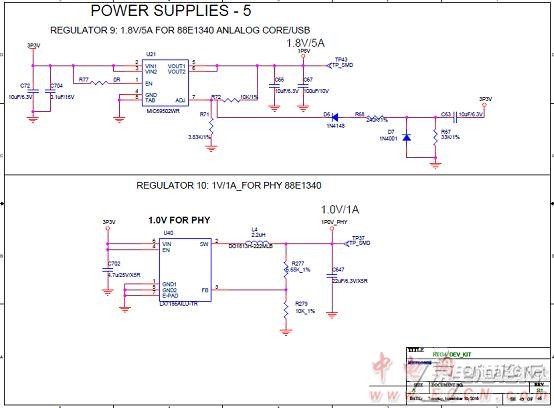
图4{京电港论坛}5.RTG4 FPGA开辟板电路原理图纸(42)

图4{京电港论坛}6.RTG4 FPGA开辟板电路原理图纸(43)
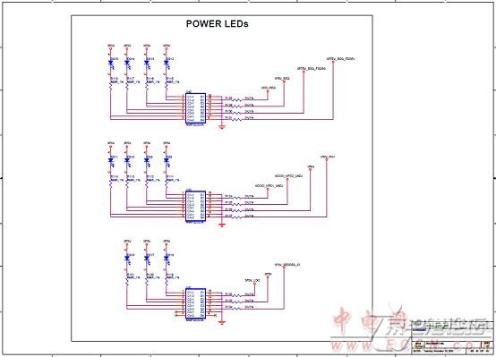
图4{京电港论坛}7.RTG4 FPGA开辟板电路原理图纸(44)
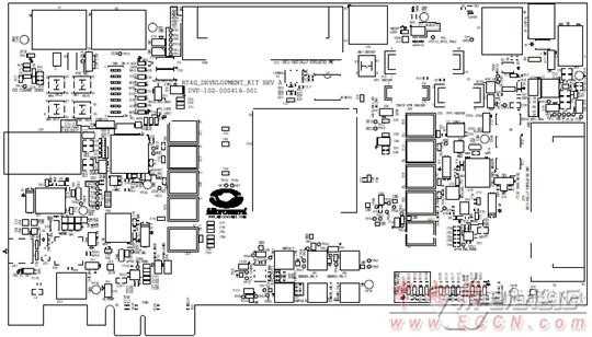
图4{京电港论坛}8.RTG4 FPGA开辟板PCB线路板元件结构图(顶层)

图4{京电港论坛}9.RTG4 FPGA开辟板PCB线路板元件结构图(底层)
RTG4 FPGA开辟板质料清单见:
 RTG4 FPGA开辟板质料清单.xls
详情请复制打开此衔接地址:
http://www.microsemi.com/products/fpga-soc/radtolerant-fpgas/rtg4#documents
 RTG4_DEV_KIT_BOARD_SCH_11-09-15_5.pdf
 ecn_dvp-102-000418-001_rtg4_dev_kit_revb_(2).zip


 热点图文
热点图文