Cypress公司的FM4 S6E2CC是基于32位ARM Cortex-M4F处理器的高度集成微控制器(MCU),集成了片上闪存和SRAM存储器,以及诸如马达控制计时器,ADC,通信接口(USB, CAN,UART, CSIO (SPI), I2C, LIN)等外设,CPU工作频率200MHz,具有性能和本钱优势,主要用在工业范畴和通信行业.本文先容了FM4 S6E2CC主要特点,框架图,以及FM4-216-ETHERNET S6E2CC开辟平台主要特点,电路图和开辟板PCB设计原理图.
Devices in the S6E2CC Series are highly integrated 32-bit microcontrollers with high performance andcompetitive cost.
This series is based on the ARM Cortex-M4F processor with on-chip flash memory and SRAM. The serieshas peripherals such as motor control timers,A/D converters, and communications interfaces (USB, CAN,UART, CSIO (SPI), I2C, LIN).
FM4 S6E2CC主要特点:
32-bit ARM Cortex-M4F Core
Processor version: r0p1
Up to 200 MHz frequency operation
FPU built-in
Support DSP instructions
Memory protection unit (MPU): improves the reliability of an embedded system
Integrated nested vectored interrupt controller (NVIC): 1 NMI (non-maskable interrupt) and 128 peripheralinterrupts and 16 priority levels
24-bit system timer (Sys Tick): system timer for OS task management
On-chip Memories
Flash memory
This series is based on two independent on-chip flash memories.
− Up to 2048 Kbytes
− Built-in flash accelerator system with 16 Kbytes trace buffer memory
− Read access to flash memory that can be achieved without wait-cycle up to an operating frequency of72 MHz. Even at the operating frequency more than 72 MHz, an equivalent single cycle access toflash memory can be obtained by the flash accelerator system.
− Security function for code protection
SRAM
This is composed of three independent SRAMs (SRAM0, SRAM1 and SRAM2). SRAM0 is connected to theI-code bus and D-code bus of Cortex-M4F core. SRAM1 and SRAM2 are connected to system bus ofCortex-M4F core.
− SRAM0: up to 192 Kbytes
− SRAM1: 32 Kbytes
− SRAM2: 32 Kbytes
External Bus Interface
Supports SRAM, NOR, NAND flash and SDRAM device
Up to 9 chip selects CS0 to CS8 (CS8 is only for SDRAM)
8-/16-/32-bit data width
Up to 25-bit address bus
Supports address/data multiplexing
Supports external RDY function
Supports scramble function
− Possible to set the validity/invalidity of the scramble function for the external areas 0x6000_0000 to
0xDFFF_FFFF in 4 Mbytes units.
− Possible to set two kinds of the scramble key
USB Interface (Max two channels)
The USB interface is composed of a function and a host.
USB function
− USB 2.0 Full-speed supported
− Max 6 EndPoint supported
− EndPoint 0 is control transfer
− EndPoint 1, 2 can be selected bulk-transfer, interrupt-transfer or isochronous-transfer
− EndPoint 3 to 5 can select bulk-transfer or interrupt-transfer
− EndPoint 1 to 5 comprise double buffer
− The size of each endpoint is as follows.
− Endpoint 0, 2 to 5: 64 byte
− EndPoint 1: 256 byte
USB host
− USB2.0 Full-Speed/Low-Speed supported
− Bulk-transfer, interrupt-transfer, and isochronous-transfer support
− USB Device connected/dis-connected automatically detect
− IN/OUT token handshake packet automatically
− Max 256-byte packet length supported
− Wake-up function supported
CAN Interface (Max two channels)
Compatible with CAN specification 2.0A/B
Maximum transfer rate: 1 Mbps
Built-in 32-message buffer
CAN-FD Interface (One channel)
Compatible with CAN Specification 2.0A/B
Maximum transfer rate: 5 Mbps
Message buffer for receiver: up to 192 messages
Message buffer for transmitter: up to 32 messages
CAN with flexible data rate (non-ISO CAN FD)
Multi-function Serial Interface (Max 16 Channels)
Separate 64 byte receive and transmit FIFO buffers for channels 0 to 7.
Operation mode is selectable for each channel from the following:
− UART
− CSIO (SPI)
− LIN
− I2C
UART
− Full-duplex double buffer
− Selection with or without parity supported
− Built-in dedicated baud rate generator
− External clock available as a serial clock
− Various error detect functions available (parity errors, framing errors, and overrun errors)
CSIO (SPI)
− Full-duplex double buffer
− Built-in dedicated baud rate generator
− Overrun error detect function available
− Serial chip select function (ch 6 and ch 7 only)
− Supports high-speed SPI (ch 4 and ch 6 only)
− Data length 5 to 16-bit
LIN
− LIN protocol Rev.2.1 supported
− Full-duplex double buffer
− Master/slave mode supported
− LIN break field generation (can change to 13- to 16-bit length)
− LIN break delimiter generation (can change to 1- to 4-bit length)
− Various error detect functions available (parity errors, framing errors, and overrun errors)
I2C
− Standard mode (Max 100 kbps)/Fast mode (Max 400 kbps) supported
− Fast mode Plus (Fm+) (Max 1000 kbps, only for ch 3 = ch A and ch 7 = ch B) supported
DMA Controller (Eight Channels)
DMA controller has an independent bus, so the CPU and DMA controller can process simultaneously.
Eight independently configured and operated channels
Transfer can be started by software or request from the built-in peripherals
Transfer address area: 32-bit (4 GB)
Transfer mode: Block transfer/Burst transfer/Demand transfer
Transfer data type: bytes/half-word/word
Transfer block count: 1 to 16
Number of transfers: 1 to 65536
DSTC (Descriptor System Data Transfer Controller; 256 channels)
The DSTC can transfer data at high-speed without going via the CPU. The DSTC adopts the descriptorsystem and, following the specified contents of the descriptor that has already been constructed on thememory, can access directly the memory/peripheral device and perform the data-transfer operation.
It supports the software activation, the hardware activation, and the chain activation functions.
A/D Converter (Max 32 Channels)
12-bit A/D Converter
− Successive approximation type
− Built-in three units
− Conversion time: 0.5 μs at 5 V
− Priority conversion available (priority at two levels)
− scanning conversion mode
− Built-in FIFO for conversion data storage (for SCAN conversion: 16 steps, for priority conversion: 4steps)
D/A Converter (Max two channels)
R-2R type
12-bit resolution
Base Timer (Max 16 channels)
Operation mode is selected from the following for each channel:
16-bit PWM timer
16-bit PPG timer
16-/32-bit reload timer
16-/32-bit PWC timer
General Purpose I/O Port
This series can use its pins as general purpose I/O ports when they are not used for external bus orperipherals; moreover, the port relocate function is built in. It can set the I/O port to which the peripheralfunction can be allocated.
Capable of pull-up control per pin
Capable of reading pin level directly
Built-in port-relocate function
Up to 120 high-speed general-purpose I/O ports in 144-pin package
Some pins 5 V tolerant I/O.
Multi-function Timer (Max three units)
The multi-function timer is composed of the following blocks:
Minimum resolution: 5.00 ns
16-bit free-run timer × 3 ch/unit
Input capture × 4 ch/unit
Output compare × 6 ch/unit
A/D activation compare × 6 ch/unit
Waveform generator × 3 ch/unit
16-bit PPG timer × 3 ch/unit
The following functions can be used to achieve the motor control:
PWM signal output function
DC chopper waveform output function
Dead time function
Input capture function
A/D convertor activate function
DTIF (motor emergency stop) interrupt function
Real-Time Clock (RTC)
The real-time clock can count year, month, day, hour, minute, second, or day of the week from 01 to 99.
Interrupt function with specifying date and time (year/month/day/hour/minute/second/day of the week) isavailable. This function is also available by specifying only year, month, day, hour, or minute.
Timer interrupt function after set time or each set time.
Capable of rewriting the time with continuing the time count.
Leap year automatic count is available.
Quadrature Position/Revolution Counter (QPRC; Max four channels)
The Quadrature Position/Revolution Counter (QPRC) is used to measure the position of the positionencoder. It is also possible to use up/down counter.
The detection edge of the three external event input pins AIN, BIN and ZIN is configurable.
16-bit position counter
16-bit revolution counter
Two 16-bit compare registers
Dual Timer (32-/16-bit Down Counter)
The dual timer consists of two programmable 32-/16-bit down counters.
Operation mode is selectable from the following for each channel:
Free-running
Periodic (= Reload)
One shot
Watch Counter
The watch counter is used for wake up from low-power consumption mode. It is possible to select the mainclock, sub clock, built-in High-speed CR clock, or built-in low-speed CR clock as the clock source.
Interval timer: up to 64 s (max) with a sub clock of 32.768 kHz
External Interrupt Controller Unit
External interrupt input pin: Max 32 pins
Include one non-maskable interrupt (NMI)
Watchdog Timer (Two channels)
A watchdog timer can generate interrupts or a reset when a time-out value is reached.
This series consists of two different watchdogs: a "hardware" watchdog and a "software" watchdog.
The hardware watchdog timer is clocked by low-speed internal CR oscillator. The hardware watchdog is thusactive in any power saving mode except RTC mode and Stop mode.
Cyclic Redundancy Check (CRC) Accelerator
The CRC accelerator helps to verify data transmission or storage integrity.
CCITT CRC16 and IEEE-802.3 CRC32 are supported.
CCITT CRC16 generator polynomial: 0x1021
IEEE-802.3 CRC32 generator polynomial: 0x04C11DB7
Programmable Cyclic Redundancy Check (PRGCRC) Accelerator
The CRC accelerator helps a verify data transmission or storage integrity.
CCITT CRC16, IEEE-802.3 CRC32 and generating polynomial are supported.
CCITT CRC16 generator polynomial: 0x1021
IEEE-802.3 CRC32 generator polynomial: 0x04C11DB7
Generating polynomial
SD Card Interface
It is possible to use the SD card that conforms to the following standards.
Part 1 Physical Layer Specification version 3.01
Part E1 SDIO Specification version 3.00
Part A2 SD Host Controller Standard Specification version 3.00
1-bit or 4-bit data bus
Ethernet-MAC
Compliant with IEEE802.3 specification
10 Mbps/100 Mbps data transfer rates supported
MII/RMII for external PHY device supported.
MII: Max one channel
RMII: Max one channel
Full-duplex and half-duplex mode supported.
Wake-ON-LAN supported
Built-in dedicated descriptor-system DMAC
Built-in 2 Kbytes transmit FIFO and 2 Kbytes receive FIFO.
Compliant IEEE1558-2008 (PTP)
I2S (Inter-IC Sound Bus) Interface (TX x one channel, RX x one channel)
Supports three transfer protocols
− I2S
− Left justified
− DSP mode
− Separate clock generation block for flexible system integration options
Master/slave mode selectable
RX Only, TX Only or TX and RX simultaneous operation selectable
Word length is programmable from 7-bits to 32-bits
RX/TX FIFO integrated (RX: 66 words x 32-bits, TX: 66 words x 32-bits)
DMA, interrupts, or polling based data transfer supported
High-speed Quad SPI
Up to 66 MHz clock rates for very fast data transfers to and from SPI compatible devices.
Up to 256 Mbytes of memory mapped address space.
Single data rate (SDR)
Supports single, dual, and quad data modes
Built-in direct mode and command sequencer mode
− Direct mode: Access by use of transmission FIFO/reception FIFO (up to16 word x 32 bit)
− Command sequencer mode: Automatic access assigned to external device area.
Clock and Reset
Clocks
Five clock sources (two external oscillators, two internal CR oscillators, and Main PLL) that are dynamicallyselectable.
− Main clock: 4 MHz to 48 MHz
− Sub clock: 30 kHz to 100 kHz
− High-speed internal CR clock: 4 MHz
− Low-speed internal CR clock: 100 kHz
− Main PLL Clock
Resets
− Reset requests from INITX pin
− Power on reset
− Software reset
− Watchdog timer reset
− Low-voltage detector reset
− Clock supervisor reset
Clock Supervisor (CSV)
Clocks generated by internal CR oscillators are used to supervise abnormality of the external clocks.
External OSC clock failure (clock stop) is detected, reset is asserted.
External OSC frequency anomaly is detected, interrupt or reset is asserted.
Low-Voltage Detector (LVD)
This Series include two-stage monitoring of voltage on the VCC pins. when the voltage falls below thevoltage that has been set, the low-voltage detector function generates an interrupt or reset.
LVD1: error reporting via interrupt
LVD2: auto-reset operation
Low-power Consumption mode
Six low power consumption modes are supported.
Sleep
Timer
RTC
Stop
Deep standby RTC (selectable from with/without RAM retention)
Deep standby stop (selectable from with/without RAM retention)
Peripheral Clock Gating
The system can reduce the current consumption of the total system with gating the operation clocks ofperipheral functions not used.
VBAT
The consumption power during the RTC operation can be reduced by supplying the power supplyindependent from the RTC (calendar circuit)/32 kHz oscillation circuit. The following circuits can also beused.
RTC
32-kHz oscillation circuit
Power-on circuit
Back up register: 32 bytes
Port circuit
Crypto Assist Function
These features are enabled for the crypto assist function.
The dedicated middleware is necessary for this calculator operation.
PKA (Public Key Accelerator)
− PKA(Public Key Accelerator)is modular exponentiation calculation accelerator used of RSA PublicKey crypto and so on.
− Available bit length: Up to 2048-bit
AES calculator
− AES (Advanced Encryption Standard) calculator is a AES common key crypto accelerator which iscompliant with FIPS (Federal Information Processing Standard Publication)197.
− Available key length: 128/192/256-bit
− CBC mode and ECB mode support
SHA-256 calculator
− SHA-256 calculator is a SHA-256 hash function accelerator which is compliant with FIPS180-2.
External Bus Data Scramble
− It enables to scramble input/output data of External Bus Interface.
Voice Function
These features are enabled for the voice function.
The dedicated library is necessary for using the voice function.
Automatic Speech Recognition (ASR)
− 100 custom commands in multiple languages
− User commands defined with a text file (no audio input or training required)
Natural Language Understanding (NLU)Debug
Serial wire JTAG debug port (SWJ-DP)
Embedded trace macrocells (ETM) provide comprehensive debug and trace facilities.
AHB trace macrocells (HTM)
Unique ID
Unique value of the device (41-bit) is set.
Power Supply
Five power supplies
− Wide range voltage: VCC = 2.7 V to 5.5 V
− Power supply for USB ch 0 I/O: USBVCC0 = 3.0 V to 3.6 V (when USB is used)
= 2.7 V to 5.5 V (when GPIO is used)
− Power supply for USB ch 1 I/O: USBVCC1 = 3.0 V to 3.6 V (when USB is used)
= 2.7 V to 5.5 V (when GPIO is used)
− Power supply for Ethernet-MAC I/O: ETHVCC = 3.0 V to 5.5 V (when Ethernet is used.)
= 2.7 V to 5.5 V (when GPIO is used)
− Power supply for VBAT: VBAT = 1.65 V to 5.5 V
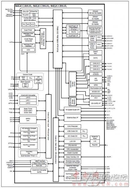
图1{京电港论坛}.FM4 S6E2CC框架图
FM4-216-ETHERNET S6E2CC开辟套件
The FM4-216-ETHERNET is a development platform for developing applications using FM4 S6E2CC MCU. This board provides a variety of peripherals for evaluating different modules of the MCU.
FM4-216-ETHERNET S6E2CC开辟板主要特点:
Microcontroller Spansion FM4 S6E2CCAL0A
FM connect Ethernet:
1x IEEE802.3 Ethernet
FM connect CAN:
2x CAN transceiver
1x CAN-FD transceiver
FM connect USB:
2x USB-Host (Type-A connector)
1x USB-Device (Type-B connector)
FM touch:
Slider using four ADC channels
FM inverter:
Motor-Control-Interface for e.g. SK-POWER-3P-LV2-MC
FM color:
Spansion S/W TFT interface (unassembled option)
Spansion flash memory S25FL164K
Connected via quad SPI interface
I2S audio interface
Using Freescale SGTL5000 audio codec
SD Card interface
Supercap for RTC power supply
1x USB-to-serial converter (Type-B connector)
Using Spansion FM3 MB9AF312K
UART and on-board JTAG simultaneously (CMSIS DAP)
Additional JTAG and Trace Interfaces each on a 20 pin-header
2x SpansionMulticon flexible serial interface
supporting I2C, SPI, UART, and LIN
User interface
Backlit LCD module
5x pushbuttons (User buttons), potentiometer
1x Reset-button, Reset-LED
Potentiometer for analog input connected to ADC
All 216 pins routed to pin-header
On-board 5V and 3V voltage regulators to supply MCU with separate Power-LEDs
4x Power supply options
USB debug port
USB-Device
JTAG
external 9V to 24V
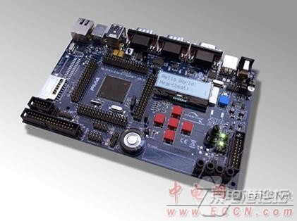
图2{京电港论坛}.FM4-216-ETHERNET S6E2CC开辟板外形图
FM4-216-ETHERNET S6E2CC开辟套件包罗:
The SK-FM4-216-ETHERNET evaluation board
USB cable
Ethernet cable
CD: Documentation, software examples and development utilities
1-page flyer
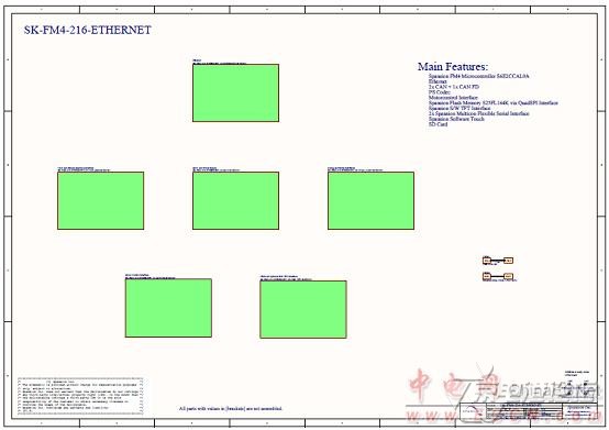
图3{京电港论坛}.FM4-216-ETHERNET S6E2CC开辟板电路图(1)

图4{京电港论坛}.FM4-216-ETHERNET S6E2CC开辟板电路图(2)
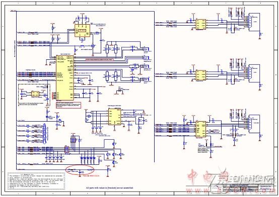
图5{京电港论坛}.FM4-216-ETHERNET S6E2CC开辟板电路图(3)
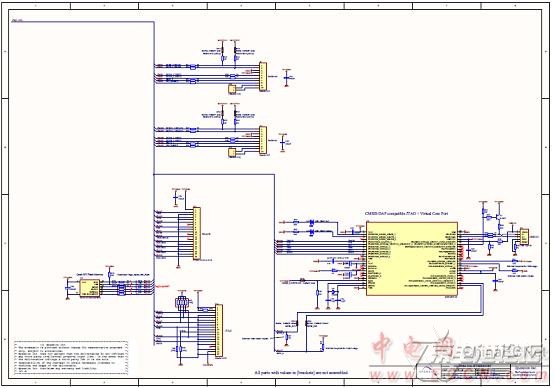
图6{京电港论坛}.FM4-216-ETHERNET S6E2CC开辟板电路图(4)
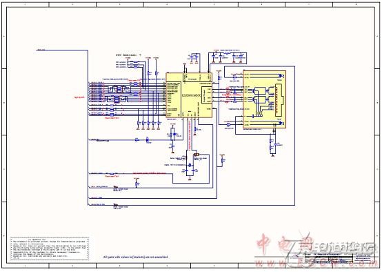
图7{京电港论坛}.FM4-216-ETHERNET S6E2CC开辟板电路图(5)
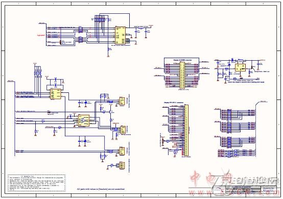
图8{京电港论坛}.FM4-216-ETHERNET S6E2CC开辟板电路图(6)
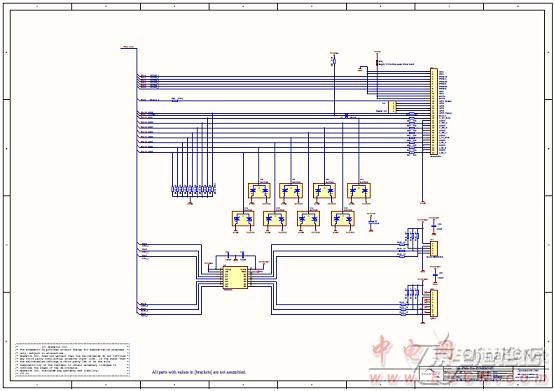
图9{京电港论坛}.FM4-216-ETHERNET S6E2CC开辟板电路图(7)
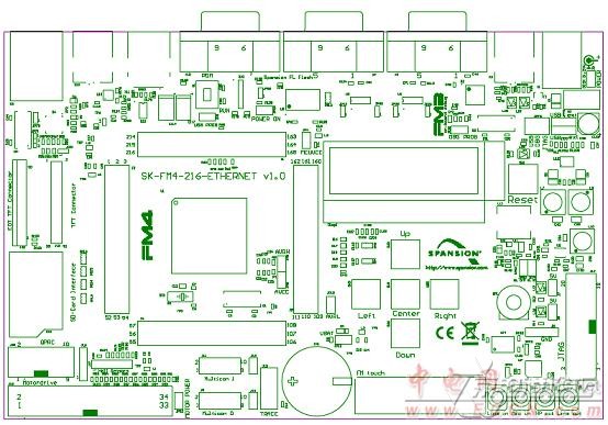
图1{京电港论坛}0.FM4-216-ETHERNET S6E2CC开辟板PCB设计原理图(1)
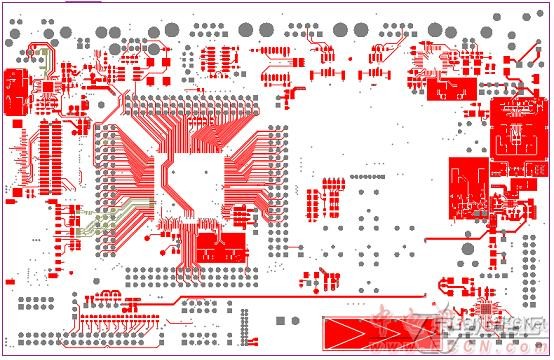
图1{京电港论坛}1.FM4-216-ETHERNET S6E2CC开辟板PCB设计原理图(2)
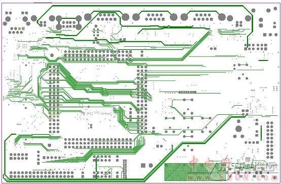
图1{京电港论坛}2.FM4-216-ETHERNET S6E2CC开辟板PCB设计原理图(3)

图1{京电港论坛}3.FM4-216-ETHERNET S6E2CC开辟板PCB设计原理图(4)
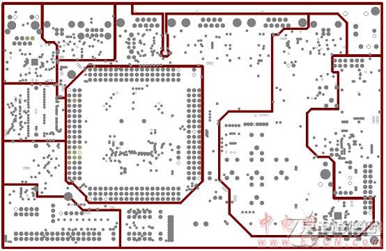
图1{京电港论坛}4.FM4-216-ETHERNET S6E2CC开辟板PCB设计原理图(5)
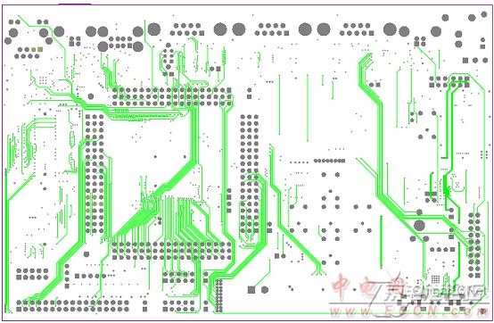
图1{京电港论坛}5.FM4-216-ETHERNET S6E2CC开辟板PCB设计原理图(6)
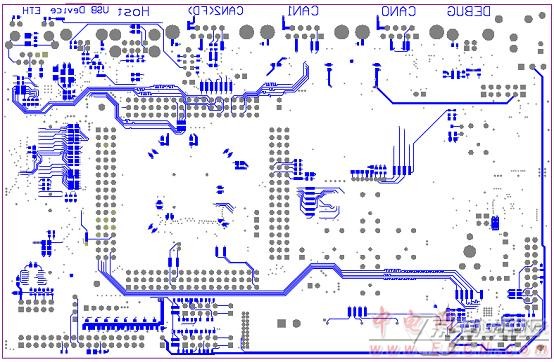
图1{京电港论坛}6.FM4-216-ETHERNET S6E2CC开辟板PCB设计原理图(7)
图1{京电港论坛}7.FM4-216-ETHERNET S6E2CC开辟板PCB设计原理图(8)
详情请复制打开此衔接地址:
http://www.spansion.com/downloads/S6E2CC_DS709-00009-E.pdf
和http://www.spansion.com/downloads/UserGuide_SK-FM4-216-ETHERNET.pdf
以及http://www.spansion.com/downloads/SK-FM4-216-ETHERNET_schematic_with_pcb.pdf
 S6E2CC_DS709-00009-E.pdf
UserGuide_SK-FM4-216-ETHERNET.pdf


 热点图文
热点图文