|
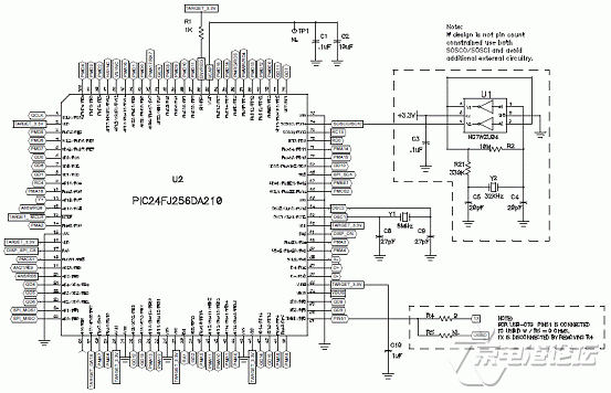
microchip 公司的PIC24FJ256DA210 是16位MCU,具有能和LCD显示器接口的图像控制器(GFX)模块,高达96KB的数据RAM。PIC24FJ256DA210高性能CPU接纳改进型哈佛架构,32MHz时的性能高达16MIPS,内部振荡器8MHz,17位x17位单周期硬件乘法器,32位x16位硬件除发器。器件工作电压2.2V-3.6V,数字输入可达5.5V。主要用在消费类电子如电热控制,无绳电话,遥控单位,家用电器,销售终端(POS)以及手提医疗设如血糖仪,血压机,手提ECG等。本京电港论坛文章先容了PIC24FJ256DA210系列主要特点,方框架图和PIC24FJ256DA210开辟板主要特点,方框架图以及详细电路原理图纸。 The PIC24FJ256DA210 family enhances on the existing line of Microchip‘s 16-bit microcontrollers, adding a new Graphics Controller (GFX) module to interface with a graphical LCD display and also adds large data RAM, up to 96 Kbytes. The PIC24FJ256DA210 family allows the CPU to fetch data directly from an external memory device using the EPMP module. PIC24FJ256DA210主要特点: Graphics Controller Features: • Three Graphics Hardware Accelerators to Facilitate Rendering of Block Copying, Text and Unpacking of Compressed Data • Color Look-up Table (CLUT) with Maximum of 256 Entries • 1/2/4/8/16 bits-per-pixel (bpp) Color Depth Set at Run Time • Display Resolution Programmable According to Frame Buffer: - Supports direct access to external memory on devices with EPMP - Resolution supported is up to 480x272 @ 60 Hz, 16 bpp; 640x480 @ 30 Hz, 16 bpp or 640x480 @ 60 Hz, 8 bpp • Supports Various Display Interfaces: - 4/8/16-bit Monochrome STN - 4/8/16-bit Color STN - 9/12/18/24-bit Color TFT (18 and 24-bit displays are connected as 16-bit, 5-6-5 RGB color format) Universal Serial Bus Features: • USB v2.0 On-The-Go (OTG) Compliant • Dual Role Capable C Can act as either Host or Peripheral • Low-Speed (1.5 Mbps) and Full-Speed (12 Mbps) USB Operation in Host mode • Full-Speed USB Operation in Device mode • High-Precision PLL for USB • Supports up to 32 Endpoints (16 bidirectional): - USB module can use the internal RAM location from 0x800 to 0xFFFF as USB endpoint buffers • On-Chip USB Transceiver with Interface for Off-Chip Transceiver • Supports Control, Interrupt, Isochronous and Bulk Transfers • On-Chip Pull-up and Pull-Down Resistors Peripheral Features: • Enhanced Parallel Master Port/Parallel Slave Port (EPMP/PSP), 100-pin devices only: - Direct access from CPU with an Extended Data Space (EDS) interface - 4, 8 and 16-bit wide data bus - Up to 23 programmable address lines - Up to 2 chip select lines - Up to 2 Acknowledgement lines (one per chip select) - Programmable address/data multiplexing - Programmable address and data Wait states - Programmable polarity on control signals • Peripheral Pin Select: - Up to 44 available pins (100-pin devices) • Three 3-Wire/4-Wire SPI modules (supports 4 Frame modes) • Three I2C™ modules Supporting Multi-Master/Slave modes and 7-Bit/10-Bit Addressing • Four UART modules: - Supports RS-485, RS-232, LIN/J2602 protocols and IrDA® • Five 16-Bit Timers/Counters with Programmable Prescaler • Nine 16-Bit Capture Inputs, each with a Dedicated Time Base • Nine 16-Bit Compare/PWM Outputs, each with a Dedicated Time Base • Hardware Real-Time Clock and Calendar (RTCC) • Enhanced Programmable Cyclic Redundancy Check (CRC) Generator • Up to 5 External Interrupt Sources High-Performance CPU • Modified Harvard Architecture • Up to 16 MIPS Operation at 32 MHz • 8 MHz Internal Oscillator • 17-Bit x 17-Bit Single-Cycle Hardware Multiplier • 32-Bit by 16-Bit Hardware Divider • 16 x 16-Bit Working Register Array • C Compiler Optimized Instruction Set Architecture with Flexible Addressing modes • Linear Program Memory Addressing, up to 12 Mbytes • Data Memory Addressing, up to 16 Mbytes: - 2K SFR space - 30K linear data memory - 66K extended data memory - Remaining (from 16 Mbytes) memory (external) can be accessed using extended data Memory (EDS) and EPMP (EDS is divided into 32-Kbyte pages) • Two Address Generation Units for Separate Read and Write Addressing of Data Memory Power Management: • On-Chip Voltage Regulator of 1.8V • Switch between Clock Sources in Real Time • Idle, Sleep and Doze modes with Fast Wake-up and Two-Speed Start-up • Run Mode: 800 A/MIPS, 3.3V Typical • Sleep mode Current Down to 20uA, 3.3V Typical • Standby Current with 32 kHz Oscillator: 22uA, 3.3V Typical Analog Features: • 10-Bit, up to 24-Channel Analog-to-Digital (A/D) Converter at 500 ksps: - Operation is possible in Sleep mode - Band gap reference input feature • Three Analog Comparators with Programmable Input/Output Configuration • Charge Time Measurement Unit (CTMU): - Supports capacitive touch sensing for touch screens and capacitive switches - Minimum time measurement setting at 100 ps • Available LVD Interrupt VLVD Level Special Microcontroller Features: • Operating Voltage Range of 2.2V to 3.6V • 5.5V Tolerant Input (digital pins only) • Configurable Open-Drain Outputs on Digital I/O Ports • High-Current Sink/Source (18 mA/18 mA) on all I/O Ports • Selectable Power Management modes: - Sleep, Idle and Doze modes with fast wake-up • Fail-Safe Clock Monitor (FSCM) Operation: - Detects clock failure and switches to on-chip, FRC oscillator • On-Chip LDO Regulator • Power-on Reset (POR) and Oscillator Start-up Timer (OST) • Brown-out Reset (BOR) • Flexible Watchdog Timer (WDT) with On-Chip Low-Power RC Oscillator for Reliable Operation • In-Circuit Serial Programming™ (ICSP™) and In-Circuit Debug (ICD) via 2 Pins • JTAG Boundary Scan Support • Flash Program Memory: - 10,000 erase/write cycle endurance (minimum) - 20-year data retention minimum - Selectable write protection boundary - Self-reprogrammable under software control - Write protection option for Configuration Words
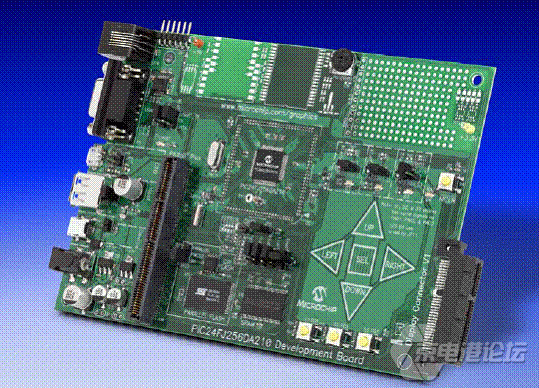
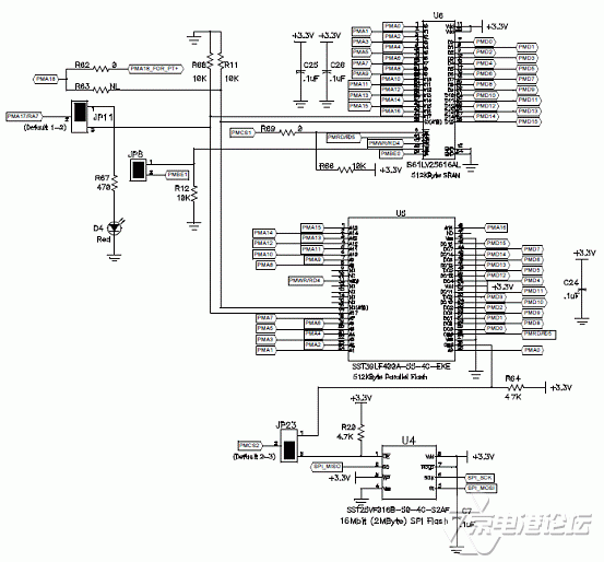
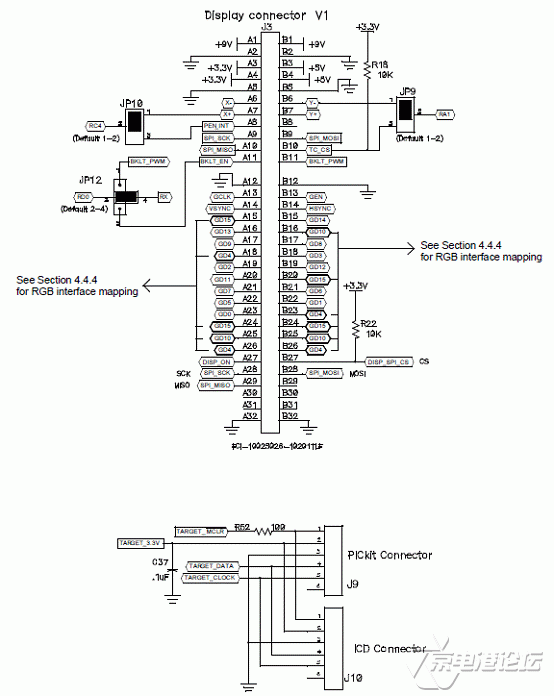
PIC24FJ256DA210开辟板 The PIC24FJ256DA210 Development Board is an efficient, low-cost development platform报to evaluate the features and performance of Microchip’s PIC24FJ256DA210 microcontroller. The 16-bit microcontroller integrates a high-performance graphics controller, CTMU and USB OTG modules essential for integrated human interface applications. Supporting this is a range of user-defined interfaces, USB options and memory expansions for the maximum flexibility in developing graphics-capable solutions. A range of Microchip development tools and software environments, along with a range of application libraries, simplifies the process of software development. Topics discussed in this chapter include: • Development Board Features • Power Requirements • Companion Display Panels • Typical Development Board Configurations • Development Board Demonstration Programs • Additional Software for Application Development
详情请复制打开此衔接地址: |


 热点图文
热点图文