|
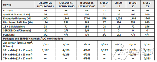
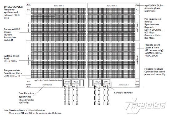
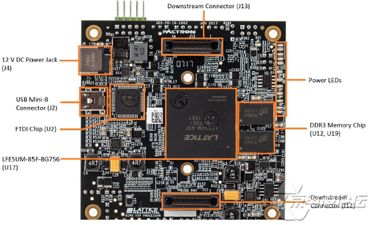
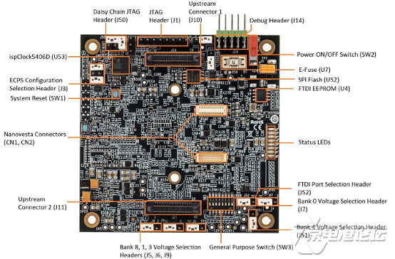
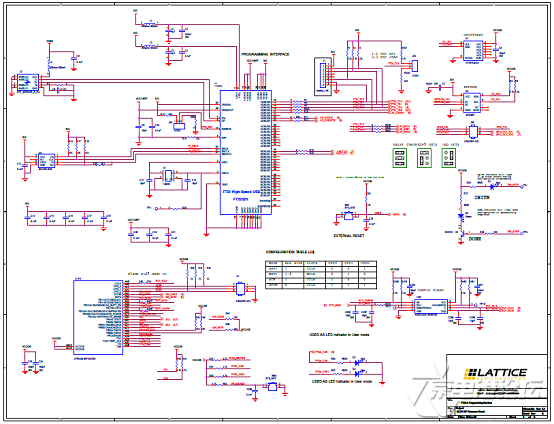
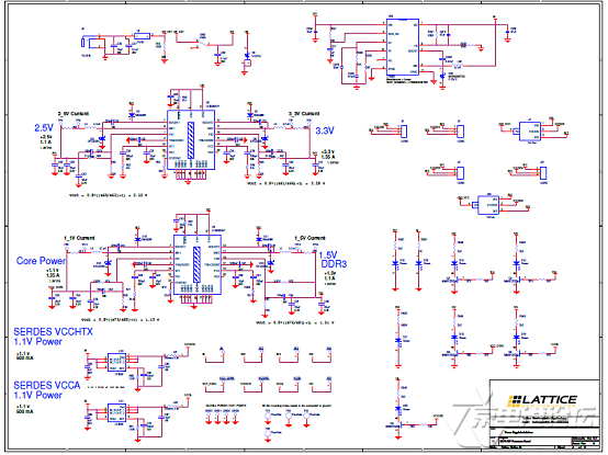
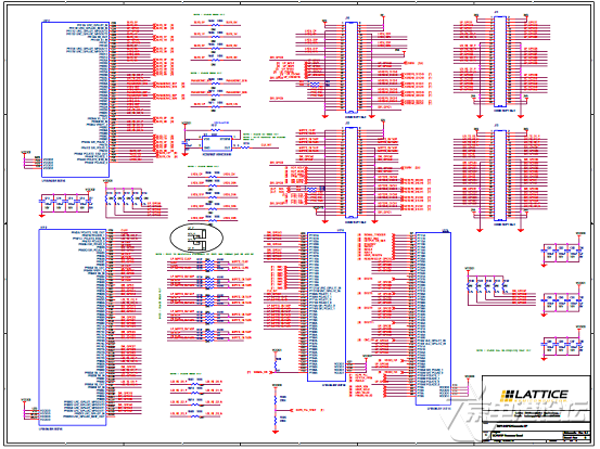
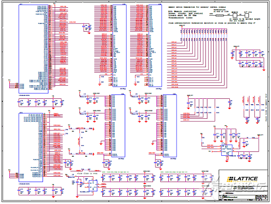
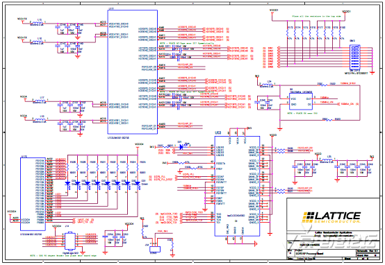
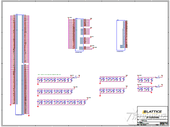
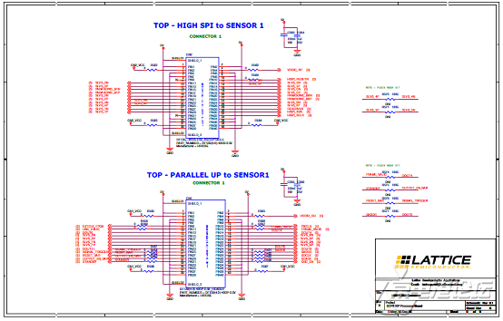
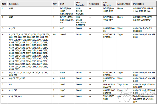
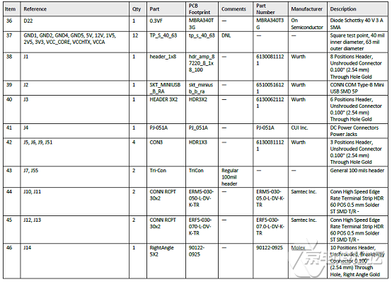
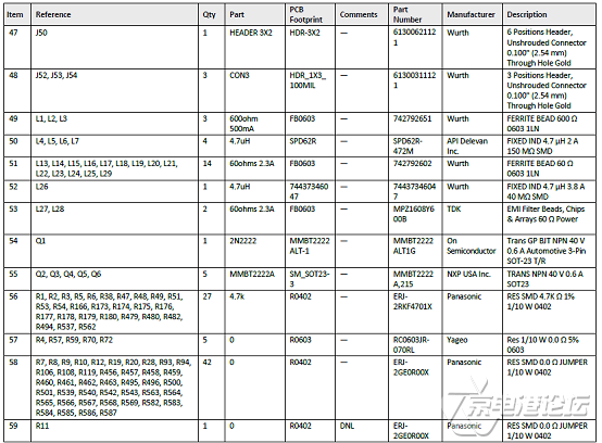
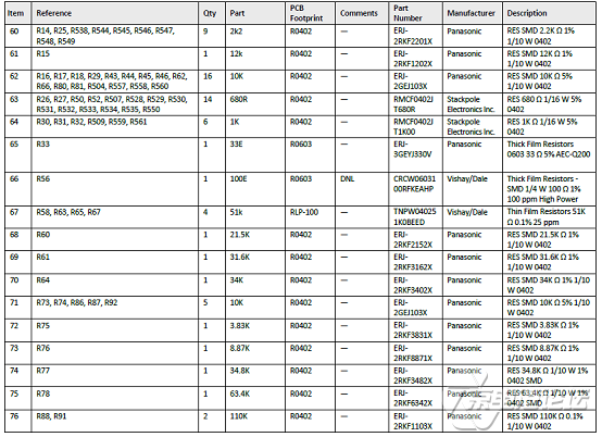
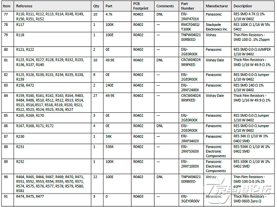
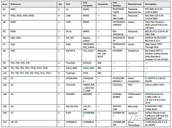
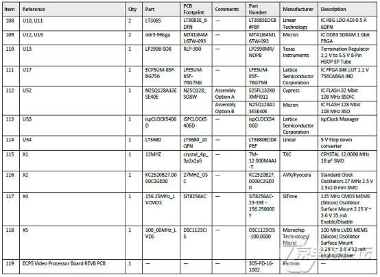
lattice公司的ECP5/ECP5-5G系列FPGA具有高性能的特性如增强的DSP架构,高速SERDES和高速源同步接口,FPGA查找表达84K逻辑单元,高达365个I/O,并提供多达156个18x18乘法器和多种并行I/O标致.采用40nm工艺技术,非常适合量大高速和低成本的应用如汽车电子和智能监测等.本文介绍了ECP5/ECP5-5G系列FPGA主要特性,系列选择表,LFE5UM/LFE5UM5G-85器件简化框图以及嵌入视频开发套板,以及ECP5 VIP处理器板主要特性和电路图与材料清单. The ECP5/ECP5-5G family of FPGA devices is optimized to deliver high performance features such as an enhanced DSP architecture, high speed SERDES and high speed source synchronous interfaces in an economical FPGA fabric. This combination is achieved through advances in device architecture and the use of 40 nm technology making the devices suitable for high-volume, high-speed, and low-cost applications. The ECP5/ECP5-5G device family covers look-up-table (LUT) capacity to 84K logic elements and supports up to 365 user I/Os. The ECP5/ECP5-5G device family also offers up to 156 18 x 18 multipliers and a wide range of parallel I/O standards. The ECP5/ECP5-5G FPGA fabric is optimized high performance with low power and low cost in mind. The ECP5/ ECP5-5G devices utilize reconfigurable SRAM logic technology and provide popular building blocks such as LUT-based logic, distributed and embedded memory, Phase Locked Loops (PLLs), Delay Locked Loops (DLLs), pre-engineered source synchronous I/O support, enhanced sysDSP slices and advanced configuration support, including encryption and dual-boot capabilities. The pre-engineered source synchronous logic implemented in the ECP5/ECP5-5G device family supports a broad range of interface standards, including DDR2/3, LPDDR2/3, XGMII and 7:1 LVDS. The ECP5/ECP5-5G device family also features high speed SERDES with dedicated Physical Coding Sublayer (PCS) functions. High jitter tolerance and low transmit jitter allow the SERDES plus PCS blocks to be configured to support an array of popular data protocols including PCI Express, Ethernet (XAUI, GbE, and SGMII) and CPRI. Transmit De-emphasis with pre- and post-cursors, and Receive Equalization settings make the SERDES suitable for transmission and reception over various forms of media. The ECP5/ECP5-5G devices also provide flexible, reliable and secure configuration options, such as dual-boot capability, bit-stream encryption, and TransFR field upgrade features. ECP5-5G family devices have made some enhancement in the SERDES compared to ECP5UM devices. These enhancements increase the performance of the SERDES to up to 5 Gb/s data rate. The ECP5-5G family devices are pin-to-pin compatible with the ECP5UM devices. These allows a migration path for users to port designs from ECP5UM to ECP5-5G devices to get higher performance. The Lattice Diamond™ design software allows large complex designs to be efficiently implemented using the ECP5/ECP5-5G FPGA family. Synthesis library support for ECP5/ECP5-5G devices is available for popular logic synthesis tools. The Diamond tools use the synthesis tool output along with the constraints from its floor planning tools to place and route the design in the ECP5/ECP5-5G device. The tools extract the timing from the routing and back-annotate it into the design for timing verification. Lattice provides many pre-engineered IP (Intellectual Property) modules for the ECP5/ECP5-5G family. By using these configurable soft core IPs as standardized blocks, designers are free to concentrate on the unique aspects of their design, increasing their productivity. ECP5 FPGA主要特性: Higher Logic Density for Increased System Integration ECP5和ECP5-5G系列选择表: 嵌入视频开发套板 This kit is pre-programmed to demonstrate the Dual CSI-2 to HDMI demo. The dual camera inputs are received by the CrossLinkpASSP, which merges into a single video stream fed to the ECP5 FPGA. The ECP5 converts the incoming image into parallel data and also performs basic image processing, and then passes it to the HDMI VIP Output Bridge Board which converts the data to HDMI format. The output can be observed on a standard HDMI monitor. 嵌入视频开发套板包括: Three-board connected kit consisting of: Embedded vision offers a promising future with many exciting new applications entering the market. These systems are used in industrial display systems for M2M applications and for Industry 4.0 implementations, Advanced Driver Assistance Systems (ADAS) and infotainment applications for automotive, DSLR cameras, drones, robotics, virtual reality (VR) systems, and medical equipment. Lattice’s product portfolio offers flexible solutions to address today’s embedded vision designer’s needs, such as evolving interface requirements, energy-efficient image signal processing and hardware acceleration. Let Lattice and its partners help you create flexible and power-efficient solutions for Embedded Vision Processing at the Edge.Embedded Vision Systems The growing implementation of cameras in almost every industry contributes towards the creation of smarter machines. Concepts like object recognition, depth perception, collision avoidance and decision making are penetrating the devices in our homes, cities, factories and cars. Computing at the Edge requires a variety of devices working together to make the machines more efficient. Consumer, industrial and automotive industries are looking at FPGAs to help them create a flexible and intelligent learning environment to realize this future. ECP5 VIP处理器板 This document describes the Lattice Semiconductor ECP5 VIP Processor Board which is a key component of Lattice’sVideo Interface Platform (VIP) board interconnect. Lattice VIP boards can be interconnected to create solutions forMIPI® CSI-2/DSI, SERDES, LVDS and more. The content of this user guide includes descriptions of onboard jumper settings, programming circuit, a complete set ofschematics, and bill of materials for ECP5 VIP processor board. ECP5 VIP处理器板主要特性:

联系我们我们在此为您提供便利。 今天我们有什么能帮到您的? 全国客服热线 :400 010 6659电话: (北京) 010-80843596 | (北京) 010-82670138 注:如需要相应技能支持,请发电邮yeguozhou@cnecport.com告示您的详细需求。  关注京电港论坛 锁定最新课程活动及技术直播 声明:京电港论坛转载作品均尽可能注明出处,该作品所有人的一切权利均不因本站而转移。 作者如不同意转载,既请通知本站予以删除或改正。转载的作品可能在标题或内容上或许有所改动。 |


 热点图文
热点图文