|
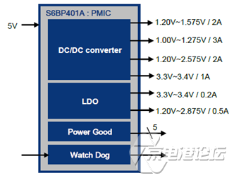
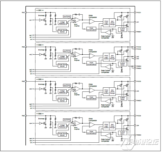
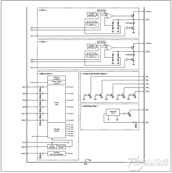
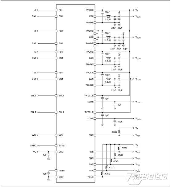
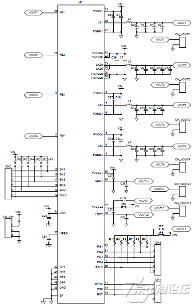
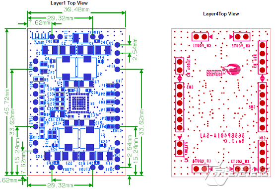
cypress公司的S6BP401A是电源管理集成电路(PMIC),包含有四个内置了开关FET的降压2.1MHz DC/DC转换器,两个低压降(LDO)的稳压器和数字窗口看门狗计时器.VIN输入电压4.5V-5.5V,内置开关FET的电流高达3A,主要用在汽车应用,先进驾驶辅助系统(ADAS),照相机系统如安全照相机和工业应用.本文介绍了S6BP401A主要特性,框图和架构框图,典型应用电路,以及评估板S6SBP401AJ0SA1001主要指标,电路图,材料清单和PCB设计图. S6BP401A is a power management IC, consists of quad buck 2.1 MHz DC/DC converter with built-in switching FETs, dual LowDrop-out regulator (LDOs) and a digital windowed watchdog timer. Having the switching FETs built-in, S6BP401A realizes highpower conversion efficiency and high switching frequency up to 2.4 MHz. The internal FETs are capable to handle up to 3A load. AsS6BP401A employs the current mode architecture, it has fast load transient response. Built-in output voltage setting resistors andcompensation circuits reduce BOM cost and component area. S6BP401A主要特性: Quad Buck DC/DC Converter (DD1 to DD4) S6BP401A应用: 评估板S6SBP401AJ0SA1001 S6SBP401AJ0SA1001 and S6SBP401AM2SA1001 are the evaluation kit for power block of automotive ADAS platform. The board implements power management IC S6BP401A. 
联系我们我们在此为您提供便利。 今天我们有什么能帮到您的? 全国客服热线 :400 010 6659电话: (北京) 010-80843596 | (北京) 010-82670138 注:如需要相应技能支持,请发电邮yeguozhou@cnecport.com告示您的详细需求。  关注京电港论坛 锁定最新课程活动及技术直播 声明:京电港论坛转载作品均尽可能注明出处,该作品所有人的一切权利均不因本站而转移。 作者如不同意转载,既请通知本站予以删除或改正。转载的作品可能在标题或内容上或许有所改动。 |


 热点图文
热点图文